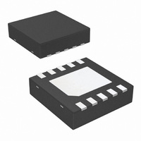
LP5996SDX-2533/NOPB National Semiconductor, LP5996SDX-2533/NOPB Datasheet

LP5996SDX-2533/NOPB
Specifications of LP5996SDX-2533/NOPB
Related parts for LP5996SDX-2533/NOPB
LP5996SDX-2533/NOPB Summary of contents
Page 1
... LDO Outputs with Independent Enable ■ 1.5% Accuracy at Room Temperature, 3% over Temperature ■ Thermal Shutdown Protection ■ Stable with Ceramic Capacitors Typical Application Circuit © 2008 National Semiconductor Corporation Key Specifications ■ Input Voltage Range ■ Low Dropout Voltage ■ Ultra-Low I ■ ...
Page 2
Functional Block Diagram Pin Descriptions Pin No Symbol 1 2 EN1 3 EN2 GND Pad GND www.national.com LLP-10 Package Name and Function V Voltage Supply Input. Connect a 1µF capacitor ...
Page 3
Connection Diagram LLP-10 Package 20171503 See NS package number SDA10A 3 www.national.com ...
Page 4
... LP5996SD-2533 LP5996SDx-2533 LP5996SD-2533 LP5996SDx-2533 2.8 2.8 LP5996SD-2828 LP5996SDX-2828 LP5996SD-2828 LP5996SDX-2828 3.0 3.0 LP5996SD-3030 LP5996SDX-3030 LP5996SD-3030 LP5996SDX-3030 3.0 3.3 LP5996SD-3033 LP5996SDX3033 LP5996SD-3033 LP5996SDX3033 3.3 0.8 LP5996SD-3308 LP5996SDX-3308 LP5996SD-3308 LP5996SDX-3308 3.3 3.3 LP5996SD-3333 LP5996SDX-3333 LP5996SD-333 LP5996SDX-3333 www.national.com Spec Package Marking NOPB L176B ...
Page 5
... Absolute Maximum Ratings (Notes Military/Aerospace specified devices are required, please contact the National Semiconductor Sales Office/ Distributors for availability and specifications. Input Voltage EN1, and EN2 -0. OUT1 OUT2 Voltage to GND Junction Temperature (T ) J-MAX Lead/Pad Temp. (Note 3) Storage Temperature Continuous Power Dissipation ...
Page 6
... Characteristics tables. Note 2: All Voltages are with respect to the potential at the GND pin. Note 3: For detailed soldering specifications and information, please refer to National Semiconductor Application Note AN-1187, Leadless Leadframe Package. Note 4: Internal thermal shutdown circuitry protects the device from permanent damage. ...
Page 7
Typical Performance Characteristics 1.0µF Ceramic 10nF, V OUT2 BYP tied Output Voltage Change vs Temperature Ground Current vs Load Current, LDO2 Dropout Voltage vs I LOAD Unless otherwise specified ...
Page 8
Line Transient, C Load Transient, LDO1 Noise Density, LDO1 www.national.com = 10nF BYP 20171519 20171550 20171556 8 Line Transient BYP 20171520 Load Transient, LDO2 20171551 Noise Density, LDO2 20171557 ...
Page 9
Short Circuit Current, LDO1 20171552 Power Supply Rejection Ratio, LDO1 20171555 Enable Start-up Time BYP 20171560 Short Circuit Current, LDO2 Power Supply Rejection Ratio, LDO2 Enable Start-up Time 20171553 20171554 = 10nF BYP 20171561 www.national.com ...
Page 10
Application Hints OPERATION DESCRIPTION The LP5996 is a low quiescent current, power management IC, designed specifically for portable applications requiring minimum board space and smallest components. The LP5996 contains two independently selectable LDOs. The first is capable of sourcing 150mA ...
Page 11
ENABLE CONTROL The LP5996 features active high enable pins for each regu- lator, EN1 and EN2, which turns the corresponding LDO ...
Page 12
Physical Dimensions www.national.com inches (millimeters) unless otherwise noted LLP, 10 Lead, Package NS Package Number SDA10A 12 ...
Page 13
13 www.national.com ...
Page 14
... For more National Semiconductor product information and proven design tools, visit the following Web sites at: Products Amplifiers www.national.com/amplifiers Audio www.national.com/audio Clock Conditioners www.national.com/timing Data Converters www.national.com/adc Displays www.national.com/displays Ethernet www.national.com/ethernet Interface www.national.com/interface LVDS www.national.com/lvds Power Management www.national.com/power Switching Regulators www.national.com/switchers LDOs www ...


