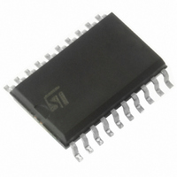
L4938ED STMicroelectronics, L4938ED Datasheet - Page 13

L4938ED
Manufacturer Part Number
L4938ED
Description
IC VREG ADVANCED DUAL SO-20
Manufacturer
STMicroelectronics
Datasheet
1.L4938EPD13TR.pdf
(20 pages)
Specifications of L4938ED
Regulator Topology
Positive Fixed and Adjustable
Voltage - Output
5V, 4.9 ~ 5.1 V
Voltage - Input
Up to 28V
Voltage - Dropout (typical)
0.2V @ 100mA, 0.3V @ 400mA
Number Of Regulators
2
Current - Output
100mA, 400mA
Current - Limit (min)
100mA, 450mA
Operating Temperature
-40°C ~ 150°C
Mounting Type
Surface Mount
Package / Case
20-SOIC (7.5mm Width)
Polarity
Positive
Number Of Outputs
2
Output Type
Fixed
Output Voltage
5 V
Output Current
5 mA
Line Regulation
20 mV
Load Regulation
50 mV
Dropout Voltage (max)
0.2 V
Input Voltage Max
20 V
Maximum Operating Temperature
+ 150 C
Minimum Operating Temperature
- 40 C
Maximum Power Dissipation
875 mW
Mounting Style
SMD/SMT
Reference Voltage
1.23 V
Voltage Regulation Accuracy
2 %
Lead Free Status / RoHS Status
Lead free / RoHS Compliant
Available stocks
Company
Part Number
Manufacturer
Quantity
Price
Part Number:
L4938ED
Manufacturer:
ST
Quantity:
20 000
Company:
Part Number:
L4938ED013TR
Manufacturer:
OKISEMICONDUCTOR
Quantity:
2 854
Part Number:
L4938ED013TR
Manufacturer:
ST
Quantity:
20 000
Part Number:
L4938EDTR-E
Manufacturer:
ST
Quantity:
20 000
L4938ED, L4938EPD
3.5
3.6
3.7
The value of the programming resistor R
The reset pulse delay time t
The reaction time of the reset circuit originates from the noise immunity. Standby output
voltage drops below the reset threshold only a bit longer than the reaction time results in a
shorter reset delay time. The nominal reset delay time is generated for standby output
voltage drops longer than approximately 50 µs. The minimum reset time is generated if reset
condition only occurs for a short time triggering a reset pulse but not completely discharging
C
capacitor are required a resistors from pin C
We recommended the use of 10 KΩ to 5 V as an output pull up.
Sense comparator
The sense comparator compares an input signal with an internal voltage reference of typical
1.23 V. The use of an external voltage divider makes this comparator very flexible in the
application. It can be used to supervise the input voltage either before or after the protection
diode and to give additional information to the microprocessor like low voltage warnings. We
recommended the use of 10 KΩ to 5 V as an output pull up.
Thermal protection
Both outputs are provided with an overtemperature shutdown regulation power dissipation
down to uncritical values. Output 2 shuts down approximately 10 K before output 1. Under
normal conditions shutdown of output 2 allows the chip to cool down again. Thus output 1 is
unaffected. The thermal shutdown reduces the output voltages until power dissipation and
the flow of thermal energy out of the chip balance.
Transient sensitivity
In proper operation (V
sensitivity to input transients.
a. The reference is alternatively supplied from V
T
. The reset can be related to output2 on request. If higher charge currents for the reset
OUT
> 4.5 V) the reference is supplied by V
RD
, is defined with the charge time of an external capacitor C
Doc ID 17243 Rev 1
R
PR
t
t
RDnom
RDmin
3.8V
=
S
PR
or V
--------------------- - 92.9K
4.7K
----------- - 1
V
≤
RT
22K
V
can be calculated with:
T
=
=
OUT1
RT
to OUT1, may be used to increase the current.
C
------------------------
C
------------------------
–
T
. If one supply is present, the reference is operating.
≤
T
1μA
1μA
⋅
⋅
4.7V
–
0.6V
1.4V
OUT1
Application information
thus reducing
13/20
T
:


