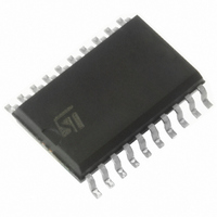
L4949EP STMicroelectronics, L4949EP Datasheet - Page 6

L4949EP
Manufacturer Part Number
L4949EP
Description
IC VREG VLDO MULTIFUNCT SO-SO2
Manufacturer
STMicroelectronics
Datasheet
1.L4949ED013TR.pdf
(19 pages)
Specifications of L4949EP
Regulator Topology
Positive Fixed
Voltage - Output
5V
Voltage - Input
Up to 28V
Voltage - Dropout (typical)
0.3V @ 100mA
Number Of Regulators
1
Current - Output
100mA
Current - Limit (min)
120mA
Operating Temperature
-40°C ~ 125°C
Mounting Type
Surface Mount
Package / Case
20-SOIC (7.5mm Width)
Number Of Outputs
1
Polarity
Positive
Input Voltage Max
28 V
Output Voltage
5 V
Output Type
Fixed
Dropout Voltage (max)
0.5 V
Output Current
100 mA
Line Regulation
20 mV
Load Regulation
30 mV
Voltage Regulation Accuracy
1 %
Maximum Operating Temperature
+ 150 C
Mounting Style
SMD/SMT
Minimum Operating Temperature
- 40 C
Reference Voltage
1.23 V
Lead Free Status / RoHS Status
Lead free / RoHS Compliant
Available stocks
Company
Part Number
Manufacturer
Quantity
Price
Part Number:
L4949EP
Manufacturer:
ST
Quantity:
20 000
Part Number:
L4949EP013TR
Manufacturer:
ST
Quantity:
20 000
Company:
Part Number:
L4949EPTR-E
Manufacturer:
ST
Quantity:
13 200
Part Number:
L4949EPTR-E
Manufacturer:
ST
Quantity:
20 000
Block diagram and pin description
6/19
Table 2.
SO-8
1
2
3
4
5
6
7
8
-
Pin N°
3, 8, 9, 13, 18
4, 5, 6, 7, 14,
15, 16, 17
SO-20
Pin definitions and functions
19
20
10
11
12
1
2
Symbol
V
GND
RES
NC
S
V
V
C
OUT
S
S
O
Z
T
I
Doc ID 4275 Rev 6
Input supply voltage. Block to GND via an external
capacitor (see
Sense input pin to supervise input voltage. Connect via an
external voltage divider connected to V
Preregulator output voltage. For details, see
Preregulator.
Reset pulse delay adjustment. Connecting this pin via a
capacitor to GND
Ground reference
Reset output. It is pulled down when the output voltage
goes below V
Sense output. This open collector pin must be connected to
V
the S
Output voltage. Block to GND via an external capacitor (see
Figure
Not connected pins
OUT
I
via an external resistor. It is pulled down whenever
voltage becomes lower than an internal voltage.
3)
RT
Figure
.
3).
Function
S
and to GND.
Section 3.4:
L4949E


