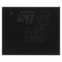
ST2L05R3300PS STMicroelectronics, ST2L05R3300PS Datasheet

ST2L05R3300PS
Specifications of ST2L05R3300PS
ST2L05R3300PS
Available stocks
Related parts for ST2L05R3300PS
ST2L05R3300PS Summary of contents
Page 1
V = 1.5, 1.8, 2.5, 2.8, 3.0, 3.3V FIXED 1.5, 1.8, 2.5, 2.8, 3.0, 3.3V FIXED OR O2 ADJUSTABLE FROM 1. GUARANTEED OUTPUT1 CURRENT: 1A GUARANTEED OUTPUT2 CURRENT: 1A ± 2% OUTPUT TOLERANCE (AT 25°C) ...
Page 2
ST2L05 BLOCK DIAGRAM OF FIXED/FIXED VERSION 2/24 ...
Page 3
... ST2L05R3315PS (*) ST2L05R3318PT ST2L05R3318PS (*) ST2L05R3325PT ST2L05R3325PS ST2L05R3328PT (*) ST2L05R3328PS (*) ST2L05R3330PT (*) ST2L05R3330PS (*) ST2L05R3333PT (*) ST2L05R3333PS (*) ST2L05R3300PT ST2L05R3300PS ST2L05 (1) SHIPMENT Tape & Reel Tape & Reel Tape & Reel Tape & Reel Tape & Reel Tape & Reel Tape & Reel Tape & Reel Tape & Reel Tape & ...
Page 4
ST2L05 ABSOLUTE MAXIMUM RATINGS Symbol V Operating Input Voltage I P Power Dissipation D I Short Circuit Output Current - 3.3 V and adjustable output OSH T Operating Junction Temperature Range op T Storage Temperature Range stg T Lead Temperature ...
Page 5
APPLICATION CIRCUIT OF FIXED/FIXED VERSION APPLICATION CIRCUIT OF FIXED/ADJ VERSION NOTE: The regulator is designed to be stable with either tantalum or ceramic capacitors on the input and outputs. The expected values of the input and output X7R ceramic capacitors ...
Page 6
ST2L05 OUTPUT1 AND OUTPUT2 DUAL SPECIFICATION ( 4.7µ 4.7 F, otherwise specified Symbol Parameter I Quiescent Current (Fixed/ADJ) GND I Quiescent Current (Fixed/Fixed) V GND I Total Current Limit I + ...
Page 7
ELECTRICAL CHARACTERISTICS OF FIXED OUTPUT 1. 4. 4.7µ Symbol Parameter V Output Voltage 1. Output Voltage 1. Line Regulation O V Load Regulation O V ...
Page 8
ST2L05 ELECTRICAL CHARACTERISTICS OF FIXED OUTPUT 2. 4. 4.7µ Symbol Parameter V Output Voltage 2. Output Voltage 2. Line Regulation O V Load Regulation O ...
Page 9
ELECTRICAL CHARACTERISTICS OF FIXED OUTPUT 2. 4. 4.7µ Symbol Parameter V Output Voltage 2. Output Voltage 2. Line Regulation O V Load Regulation O V ...
Page 10
ST2L05 ELECTRICAL CHARACTERISTICS OF FIXED OUTPUT 3. 4. 4.7µ Symbol Parameter V Output Voltage 3. Output Voltage 3. Line Regulation O V Load Regulation O ...
Page 11
ELECTRICAL CHARACTERISTICS OF FIXED OUTPUT 3. 4. 4.7µ Symbol Parameter V Output Voltage 3. Output Voltage 3. Line Regulation O V Load Regulation O V ...
Page 12
ST2L05 ELECTRICAL CHARACTERISTICS OF ADJUSTABLE OUTPUT ( 4. 4.7µ Symbol Parameter V Reference Voltage O V Reference Voltage O V Line Regulation Load Regulation ...
Page 13
ST2L05 stability using multilayer ceramic capacitors show that a minimum value of 2.2µF is needed for both regulators. This value can be increased without limit if the input ...
Page 14
ST2L05 TYPICAL CHARACTERISTICS Figure 1 : Reference Voltage vs Temperature Figure 2 : Reference Line Regulation vs Temperature Figure 3 : Reference Load Regulation vs Temperature 14/24 Figure 4 : Reference Voltage vs Input Voltage Figure 5 : Dropout Voltage ...
Page 15
Figure 7 : Minimum Load Current vs Temperature (Adjustable Output) Figure 8 : Adjust Pin Current vs Temperature (Adjustable Output) Figure 9 : Output Voltage vs Temperature Figure 10 : Line Regulation vs Temperature Figure 11 : Load Regulation vs ...
Page 16
ST2L05 Figure 13 : Dropout Voltage vs Temperature (Fixed Output) Figure 14 : Dropout Voltage vs Input Voltage Figure 15 : Supply Voltage Rejection vs Temperature 16/24 Figure 16 : Supply Voltage Rejection vs Frequency Figure 17 : Quiescent Current ...
Page 17
Figure 19 : Short Circuit Removal Response V =5V, I =short circuit to 10mA X5R, T =25°C J Figure 20 : Change of V with Step Load O Change V =5V, I =1mA ...
Page 18
ST2L05 Figure 25 : Change of V with Step Load O Change V =5V, I =1mA to 1A =22 F all ceramic X5R =25° =1µs J RISE FALL Figure ...
Page 19
SPAK-5L MECHANICAL DATA DIM. MIN. A 1. 1.02 D1 7. 9.27 H3 8.89 L 10. 8. 3˚ mm. TYP MAX. MIN. 2.03 0.070 ...
Page 20
ST2L05 DIM. MIN. A 2.2 A1 0.9 A2 0.03 B 0.4 B2 5.2 C 0. 6.4 G 4.9 G1 2. 0.6 20/24 PPAK MECHANICAL DATA mm. TYP MAX. 2.4 1.1 0.23 ...
Page 21
DFN8 (5x6) MECHANICAL DATA mm. DIM. MIN 0.219 L 0.70 TYP MAX. MIN. 0.90 1.00 0.032 0.02 0.005 0.20 0.40 0.47 0.014 5.00 ...
Page 22
ST2L05 Tape & Reel SPAK-xL MECHANICAL DATA DIM. MIN 12 9.70 Bo 10.85 Ko 2.30 Po 3.9 P 11.9 22/24 mm. TYP MAX. 180 13.0 13.2 14.4 9.80 9.90 10.95 11.05 2.40 ...
Page 23
Tape & Reel DPAK-PPAK MECHANICAL DATA DIM. MIN 12 6.80 Bo 10.40 10.50 Ko 2.55 Po 3.9 P 7.9 mm. TYP MAX. MIN. 330 13.0 13.2 0.504 0.795 2.362 14.4 6.90 7.00 ...
Page 24
... No license is granted by implication or otherwise under any patent or patent rights of STMicroelectronics. Specifications mentioned in this publication are subject to change without notice. This publication supersedes and replaces all information previously supplied ...


