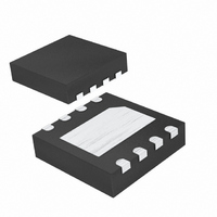
MAX5091BATA+T Maxim Integrated Products, MAX5091BATA+T Datasheet - Page 8

MAX5091BATA+T
Manufacturer Part Number
MAX5091BATA+T
Description
IC REG LDO 3.3V 8-TDFN
Manufacturer
Maxim Integrated Products
Datasheet
1.MAX5091BATAT.pdf
(15 pages)
Specifications of MAX5091BATA+T
Regulator Topology
Positive Fixed
Voltage - Output
3.3V
Voltage - Input
5 ~ 28 V
Voltage - Dropout (typical)
0.3V @ 100mA
Number Of Regulators
1
Current - Output
100mA
Current - Limit (min)
160mA
Operating Temperature
-40°C ~ 125°C
Mounting Type
Surface Mount
Package / Case
8-TDFN Exposed Pad
Number Of Outputs
1
Polarity
Positive
Input Voltage Max
28 V
Output Voltage
3.3 V
Output Type
Fixed
Dropout Voltage (max)
0.25 V at 10 mA
Output Current
100 mA
Line Regulation
5 mV
Load Regulation
40 mV
Maximum Power Dissipation
1.951 W
Maximum Operating Temperature
+ 125 C
Mounting Style
SMD/SMT
Minimum Operating Temperature
- 40 C
Lead Free Status / RoHS Status
Lead free / RoHS Compliant
Other names
MAX5091BATA+T
MAX5091BATA+TTR
MAX5091BATA+TTR
28V, 100mA, Low-Quiescent-Current LDO
with Reset and Power-Fail Input/Output
8
(Typical Application Circuit, V
wise noted.)
0V
0V
PIN
EP
_______________________________________________________________________________________
1
2
3
4
5
6
7
8
V
OUT
NAME
V
GND
RES
EN
SO
STARTUP RESPONSE
CT
EP
V
OUT
SI
S
10ms/div
Regulator Input. Operating supply range is from +5V to +28V and withstands 40V transients. Bypass
V
Voltage Sense/Power-Fail Comparator Input. SI is the noninverting input of an uncommitted comparator. SO
asserts low if V
Enable Input. Leave unconnected (or pull EN high) to turn on the regulator. Pull EN low to place the device in
shutdown mode. EN is internally pulled up to 3.6V.
Reset Timeout Delay Capacitor Connection. Connect a capacitor from CT to GND to program the reset
timeout period/reset pulse delay. During regulation, CT is pulled up to V
when EN is low, or when in thermal shutdown.
Ground. Bypass the input and output capacitors to the GND plane. Solder to large pads or the circuit-board
ground plane to maximize thermal dissipation.
Active-Low Reset Output. Pull up externally to V
threshold. Once output voltage is in regulation, RES goes high after the programmed reset timeout period is
over. RES is low when EN is low or in thermal shutdown.
Voltage Sense/Power-Fail Comparator Output. Pull up externally to V
low when V
shutdown.
Regulator Output. Fixed at +5V (MAX5091A) or +3.3V (MAX5091B). Bypass with a 10µF ceramic capacitor to
GND.
E xp osed P ad d l e. E P i s i nter nal l y connected to GN D . C onnect E P to GN D to p r ovi d e a l ow ther m al - r esi stance
p ath fr om the IC j uncti on to the P C b oar d . D o not use as the onl y el ectr i cal connecti on to G N D .
S
to GND with a 10µF capacitor.
I
OUT
S
MAX5091 toc21
= 10mA
= +14V, C
SI
drops below the reference level, V
SI
V
2V/div
V
5V/div
OUT
S
drops below the reference level, V
IN
= 10µF, C
0V
0V
Typical Operating Characteristics (continued)
OUT
ENABLE RESPONSE
= 10µF, V
200μs/div
OUT
SI
ST
FUNCTION
. SO also asserts low when EN is low or in thermal
= 0V, V
ST
. Open-drain RES goes low when V
I
OUT
.
MAX5091 toc22
= 100mA
EN
= +2.4V, V
V
5V/div
EN
5V/div
OUT
OUT
OUT
OUT
. Open-drain SO asserts
. CT is pulled low during reset,
= +5V, T
SHUTDOWN RESPONSE
Pin Description
200μs/div
A
OUT
= +25°C, unless other-
is below the reset
I
OUT
= 100mA
MAX5091 toc23
V
2V/div
EN
2V/div
0V
0V
OUT


