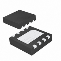
MAX5091BATA+T Maxim Integrated Products, MAX5091BATA+T Datasheet - Page 11

MAX5091BATA+T
Manufacturer Part Number
MAX5091BATA+T
Description
IC REG LDO 3.3V 8-TDFN
Manufacturer
Maxim Integrated Products
Datasheet
1.MAX5091BATAT.pdf
(15 pages)
Specifications of MAX5091BATA+T
Regulator Topology
Positive Fixed
Voltage - Output
3.3V
Voltage - Input
5 ~ 28 V
Voltage - Dropout (typical)
0.3V @ 100mA
Number Of Regulators
1
Current - Output
100mA
Current - Limit (min)
160mA
Operating Temperature
-40°C ~ 125°C
Mounting Type
Surface Mount
Package / Case
8-TDFN Exposed Pad
Number Of Outputs
1
Polarity
Positive
Input Voltage Max
28 V
Output Voltage
3.3 V
Output Type
Fixed
Dropout Voltage (max)
0.25 V at 10 mA
Output Current
100 mA
Line Regulation
5 mV
Load Regulation
40 mV
Maximum Power Dissipation
1.951 W
Maximum Operating Temperature
+ 125 C
Mounting Style
SMD/SMT
Minimum Operating Temperature
- 40 C
Lead Free Status / RoHS Status
Lead free / RoHS Compliant
Other names
MAX5091BATA+T
MAX5091BATA+TTR
MAX5091BATA+TTR
The MAX5091 high-voltage regulator provides up to
100mA of output current. The input voltage extends to
+28V. Package power dissipation limits the amount of
output current available for a given input/output voltage
and ambient temperature. Figure 2 depicts the maxi-
mum power dissipation curve for the 8-pin SO-EP pack-
age. The graph assumes that the exposed metal back
of the MAX5091 package is soldered to copper on a
single layer PCB according to the JEDEC51 standard.
Use Figure 2 to determine the allowable package dissi-
pation for a given ambient temperature. Alternately, use
the following formula to calculate the allowable pack-
age dissipation:
Figure 2. 8-Pin SO-EP Maximum Power Dissipation vs.
Temperature
P
D
=
⎧
⎨
⎩
1.538 0.01923 T
Available Output Current Calculation
2.0
1.8
1.6
1.4
1.2
1.0
0.8
0.6
0.4
0.2
0
−
10
Applications Information
28V, 100mA, Low-Quiescent-Current LDO
20
1.538W
______________________________________________________________________________________
30
(
1.538W For T
with Reset and Power-Fail Input/Output
40
A
TEMPERATURE (°C)
50
−
70
60
°
70
C For
)
80
90
A
100
19.23mW/°C
+
110
8-PIN SO-EP
DERATE
≤ +
70 C
120
°
70 C
130
°
140
<
150
T
A
≤ +
125 C
°
After determining the allowable package dissipation, cal-
culate the maximum output current using the following
formula:
The above equations do not include the power dissipation
from self-heating due to the IC ground current.
The junction-to-ambient thermal impedance depends
on the area of the copper plane, its thickness, and the
number of copper layers on PCB. For the higher power
dissipation requirement, use multiple-layered PCBs
with 2oz copper and a large copper area.
For stable operation over the full temperature range and
with load currents up to 100mA, use a 10µF output
capacitor with a low ESR. Table 1 shows a list of recom-
mended output capacitor ESR for various load conditions.
Table 1. Recommended Output Capacitor
ESR
I
I
I
OUT
OUT
OUT
I
≤ 100mA
OUT
≤ 10mA
≤ 50mA
I
OUT(MAX)
RECOMMENDED C
C
C
C
V
ESR
ESR
ESR
OUT
≅
Capacitor Selection and
< 0.132Ω
V
< 0.66Ω
< 66mΩ
= 3.3V
S
−
Regulator Stability
P
D
OUT
V
OUT
ESR
V
C
C
C
OUT
ESR
ESR
ESR
< 0.2Ω
< 0.1Ω
= 5.0V
< 1Ω
11


