LP38853MR-ADJ/NOPB National Semiconductor, LP38853MR-ADJ/NOPB Datasheet - Page 3
LP38853MR-ADJ/NOPB
Manufacturer Part Number
LP38853MR-ADJ/NOPB
Description
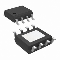
IC REG LDO 3A ADJ OUT 8-PSOP
Manufacturer
National Semiconductor
Series
PowerWise®r
Datasheet
1.LP38853EVAL.pdf
(18 pages)
Specifications of LP38853MR-ADJ/NOPB
Regulator Topology
Positive Adjustable
Voltage - Output
0.8 ~ 1.8 V
Voltage - Input
1.04 ~ 5.5 V
Voltage - Dropout (typical)
0.24V @ 3A
Number Of Regulators
1
Current - Output
3A (Max)
Operating Temperature
-40°C ~ 125°C
Mounting Type
Surface Mount
Package / Case
8-PSOP
For Use With
LP38853EVAL - BOARD EVALUATION LP38853
Lead Free Status / RoHS Status
Lead free / RoHS Compliant
Current - Limit (min)
-
Other names
*LP38853MR-ADJ/NOPB
LP38853MR-ADJ
LP38853MR-ADJ
Available stocks
Company
Part Number
Manufacturer
Quantity
Price
Company:

Part Number:
LP38853MR-ADJ/NOPB
Manufacturer:
TI
Quantity:
25
Company:
Part Number:
LP38853MR-ADJ/NOPB
Manufacturer:
NS
Quantity:
1


ΔV
ΔV
ΔV
UVLO
Absolute Maximum Ratings
If Military/Aerospace specified devices are required,
please contact the National Semiconductor Sales Office/
Distributors for availability and specifications.
Electrical Characteristics
V
type apply over the junction temperature (T
test, design, or statistical correlation. Typical values represent the most likely parametric norm at T
reference purposes only.
I
Storage Temperature Range
Lead Temperature
ESD Rating
Power Dissipation (Note 3)
V
V
V
Symbol
OUT
GND(BIAS)
BIAS
I
OUT
UVLO
IN
BIAS
SS
OUT
GND(IN)
V
V
Soldering, 5 seconds
Human Body Model (Note 2)
V
I
OUT
ADJ
SC
Supply Voltage (Survival)
/ΔV
DO
SoftStart Voltage (Survival)
/ΔI
, I
/ΔV
(HYS)
Supply Voltage (Survival)
OUT
OUT
BIAS
IN
= 10 mA, C
V
V
Line Regulation, V
Line Regulation, V
Output Voltage Load Regulation
(Note 5)
Dropout Voltage (Note 6)
Quiescent Current Drawn from
V
Quiescent Current Drawn from
V
Under-Voltage Lock-Out
Threshold
Under-Voltage Lock-Out
Hysteresis
Output Short-Circuit Current
ADJ
OUT
IN
BIAS
Supply
Accuracy
Range
Supply
IN
= C
Parameter
OUT
= 10 µF, C
IN
BIAS
(Note 4)
(Note 4)
BIAS
−65°C to +150°C
Internally Limited
J
) range of -40°C to +125°C. Minimum and Maximum limits are guaranteed through
−0.3V to +6.0V
−0.3V to +6.0V
−0.3V to +6.0V
Unless otherwise specified: V
= 1 µF, C
(Note 1)
V
See (Note 7)
3.0V
10 mA
V
See (Note 7)
3.0V
10 mA
0°C
3.0V
4.5V
V
3.0V
10 mA
I
V
V
10 mA
V
10 mA
V
V
V
device is non-functional
V
V
OUT
OUT(NOM)
OUT(NOM)
OUT(NOM)
OUT
BIAS
EN
EN
BIAS
BIAS
IN
BIAS
= V
260°C
≤
≤
≤
= 3.0A
±2 kV
≤
≤
≤
≤
≤
= 0.80V
falling from UVLO threshold until
= 3.0V
rising until device is functional
= 3.0V, V
SS
T
0.5V
0.5V
≤
≤
≤
≤
≤
OUT(NOM)
V
V
V
V
V
J
= open. Limits in standard type are for T
BIAS
BIAS
BIAS
BIAS
BIAS
I
I
≤
I
I
I
+1V
+1V
+1V
OUT
OUT
OUT
OUT
OUT
+125°C
Conditions
≤
≤
≤
≤
≤
≤
≤
≤
≤
≤
≤
≤
≤
3
OUT
5.5V,
5.5V,
5.5V
5.5V
5.5V
+ 1V,
3A
3.0A,
3.0A
3.0A
3.0A
V
V
V
IN
IN
IN
Operating Ratings
= 0.0V
V
I
Junction Temperature
OUT
≤
≤
≤
V
V
V
I
Junction Temperature Range
(Note 3)
OUT
OUT
IN
BIAS
EN
V
V
V
Current (Survival)
BIAS
BIAS
BIAS
Supply Voltage
Voltage
Voltage (Survival)
OUT
0.8V
1.2V < V
Supply Voltage
≤
≤
= 0.80V, V
4.5V,
4.5V,
≤
V
OUT
OUT
≤
≤
IN
1.8V
1.2V
492.5
485.0
490.0
0.80
0.80
2.20
2.00
= V
Min
60
50
-
-
-
-
-
-
-
OUT(NOM)
J
= 25°C only; limits in boldface
J
= 25°C, and are provided for
(Note 1)
500.
500.
0.04
0.10
2.45
Typ
240
100
150
0.2
7.0
3.0
5.8
1
+ 1V, V
(V
OUT
−40°C to +125°C
−40°C to +150°C
BIAS
Internally Limited
507.5
515.0
510.0
+ V
Max
1.20
1.80
2.70
2.90
300
450
300
170
200
300
350
−0.3V to +6.0V
8.5
9.0
3.8
4.5
10
0.0V to V
0 mA to 3.0A
-
-
-
-
3.0V to 5.5V
4.5V to 5.5V
= 3.0V, V
DO
www.national.com
) to V
Units
BIAS
BIAS
%/V
%/V
%/A
mV
mV
mA
mA
mV
μA
μA
EN
V
V
A
=
Related parts for LP38853MR-ADJ/NOPB
Image
Part Number
Description
Manufacturer
Datasheet
Request
R

Part Number:
Description:
IC, REG, LDO, 3A, POWERWISE, PSOP8
Manufacturer:
National Semiconductor
Datasheet:

Part Number:
Description:
National Semiconductor [8-Bit D/A Converter]
Manufacturer:
National Semiconductor
Datasheet:
Part Number:
Description:
National Semiconductor [Media Coprocessor]
Manufacturer:
National Semiconductor
Datasheet:
Part Number:
Description:
Digitally Controlled Tone and Volume Circuit with Stereo Audio Power Amplifier, Microphone Preamp Stage and National 3D Sound
Manufacturer:
National Semiconductor
Datasheet:
Part Number:
Description:
Digitally Controlled Tone and Volume Circuit with Stereo Audio Power Amplifier, Microphone Preamp Stage and National 3D Sound
Manufacturer:
National Semiconductor
Datasheet:
Part Number:
Description:
AC97 Rev 2 Codec with Sample Rate Conversion and National 3D Sound
Manufacturer:
National Semiconductor
Part Number:
Description:
Manufacturer:
National Semiconductor
Datasheet:
Part Number:
Description:
Manufacturer:
National Semiconductor
Datasheet:
Part Number:
Description:
General Purpose, Low Voltage, Low Power, Rail-to-Rail Output Operational Amplifiers
Manufacturer:
National Semiconductor
Datasheet:
Part Number:
Description:
8-bit 20 MSPS flash A/D converter.
Manufacturer:
National Semiconductor
Datasheet:
Part Number:
Description:
Low Noise Quad Operational Amplifier
Manufacturer:
National Semiconductor
Datasheet:
Part Number:
Description:
Quad Differential Line Receivers
Manufacturer:
National Semiconductor
Datasheet:
Part Number:
Description:
Quad High Speed Trapezoidal? Bus Transceiver
Manufacturer:
National Semiconductor
Datasheet:
Part Number:
Description:
Dual Line Receiver
Manufacturer:
National Semiconductor
Datasheet: