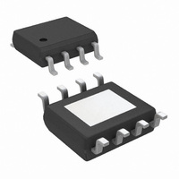
LP38853MR-ADJ/NOPB National Semiconductor, LP38853MR-ADJ/NOPB Datasheet - Page 13

LP38853MR-ADJ/NOPB
Manufacturer Part Number
LP38853MR-ADJ/NOPB
Description
IC REG LDO 3A ADJ OUT 8-PSOP
Manufacturer
National Semiconductor
Series
PowerWise®r
Datasheet
1.LP38853EVAL.pdf
(18 pages)
Specifications of LP38853MR-ADJ/NOPB
Regulator Topology
Positive Adjustable
Voltage - Output
0.8 ~ 1.8 V
Voltage - Input
1.04 ~ 5.5 V
Voltage - Dropout (typical)
0.24V @ 3A
Number Of Regulators
1
Current - Output
3A (Max)
Operating Temperature
-40°C ~ 125°C
Mounting Type
Surface Mount
Package / Case
8-PSOP
For Use With
LP38853EVAL - BOARD EVALUATION LP38853
Lead Free Status / RoHS Status
Lead free / RoHS Compliant
Current - Limit (min)
-
Other names
*LP38853MR-ADJ/NOPB
LP38853MR-ADJ
LP38853MR-ADJ
Available stocks
Company
Part Number
Manufacturer
Quantity
Price
Company:
Part Number:
LP38853MR-ADJ/NOPB
Manufacturer:
TI
Quantity:
25
Company:
Part Number:
LP38853MR-ADJ/NOPB
Manufacturer:
NS
Quantity:
1
10X difference in leakage between 25°C and 85°C, so the
maximum ambient temperature must be included in the ca-
pacitor selection process.
Typical C
providing typical Soft-Start times in the range of 70 μs to 7 ms
(5τ). Values less than 1 nF can be used, but the Soft-Start
effect will be minimal. Values larger than 100 nF will provide
soft-start, but may not be fully discharged if V
the UVLVO threshold to less than 500 mV in less than 100
µs.
Figure 2 shows the relationship between the C
a typical C
The C
back to the device ground pin. No components, other than
C
adverse effects to V
If the Soft-Start function is not needed the SS pin should be
left open, although some minimal capacitance value is always
recommended.
ENABLE OPERATION
The Enable pin (EN) provides a mechanism to enable, or dis-
able, the regulator output stage. The Enable pin has an
internal pull-up, through a typical 180 kΩ resistor, to V
If the Enable pin is actively driven, pulling the Enable pin
above the V
lator output on, while pulling the Enable pin below the V
threshold will turn the regulator output off. There is approxi-
mately 100 mV of hysteresis built into the Enable threshold
provide noise immunity.
If the Enable function is not needed this pin should be left
open, or connected directly to V
open, stray capacitance on this pin must be minimized, oth-
erwise the output turn-on will be delayed while the stray
capacitance is charged through the internal resistance (r
POWER DISSIPATION AND HEAT-SINKING
Additional copper area for heat-sinking may be required de-
pending on the maximum device dissipation (P
maximum anticipated ambient temperature (T
vice. Under all possible conditions, the junction temperature
must be within the range specified under operating condi-
tions.
SS
, should be connected to the SS pin, as there could be
SS
capacitor must be connected to a clean ground path
SS
FIGURE 2. Typical C
SS
EN
values will be in the range of 1 nF to 100 nF,
value.
threshold of 1.25V (typical) will turn the regu-
OUT
.
SS
BIAS
vs C
. If the Enable pin is left
OUT
Values
BIAS
OUT
A
20131023
) for the de-
D
value and
) and the
falls from
BIAS
EN
.
EN
).
13
The total power dissipation of the device is the sum of three
different points of dissipation in the device.
The first part is the power that is dissipated in the NMOS pass
element, and can be determined with the formula:
The second part is the power that is dissipated in the bias and
control circuitry, and can be determined with the formula:
where I
of the device that is related to V
The third part is the power that is dissipated in portions of the
output stage circuitry, and can be determined with the formu-
la:
where I
of the device that is related to V
The total power dissipation is then:
The maximum allowable junction temperature rise (ΔT
pends on the maximum anticipated ambient temperature
(T
junction temperature (T
The maximum allowable value for junction to ambient Ther-
mal Resistance, θ
Heat-Sinking The TO-220 Package
The TO220-5 package has a θ
rating of 3°C/W. These ratings are for the package only, no
additional heat-sinking, and with no airflow. If the needed
θ
then no additional heat-sinking is required since the package
can safely dissipate the heat and not exceed the operating
T
heat-sinking is needed.
The thermal resistance of a TO-220 package can be reduced
by attaching it to a heat sink or a copper plane on a PC board.
If a copper plane is to be used, the values of θ
as shown in next section for TO-263 package.
The heat-sink to be used in the application should have a
heat-sink to ambient thermal resistance, θ
where θ
junction to the ambient air, θ
the case to the surface of the heart-sink, and θ
resistance from the junction to the surface of the case.
JA
J(MAX)
A
) for the application, and the maximum allowable operating
, as calculated above, is greater than or equal to 60°C/W
. If the needed θ
GND(BIAS)
GND(IN)
JA
is the required total thermal resistance from the
P
P
D
P
D(PASS)
is the portion of the operating ground current
= P
D(BIAS)
is the portion of the operating ground current
P
JA
D(PASS)
D(IN)
, can be calculated using the formula:
= (V
= V
= V
JA
J(MAX)
BIAS
+ P
is less than 60°C/W then additional
IN
IN
- V
CH
× I
) .
D(BIAS)
× I
OUT
JA
is the thermal resistance from
GND(IN)
BIAS
IN
GND(BIAS)
.
rating of 60°C/W and a θ
) × I
.
+ P
OUT
D(IN)
HA
:
JC
JA
is the thermal
will be same
www.national.com
J
) de-
(10)
(11)
(12)
(13)
(14)
(8)
(9)
JC


