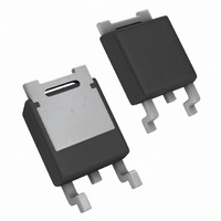
LP38690DT-5.0/NOPB National Semiconductor, LP38690DT-5.0/NOPB Datasheet - Page 3

LP38690DT-5.0/NOPB
Manufacturer Part Number
LP38690DT-5.0/NOPB
Description
IC REG LDO 1A 5.0V TO-252
Manufacturer
National Semiconductor
Series
PowerWise®r
Type
Voltage Regulatorr
Datasheet
1.LP38690DT-5.0NOPB.pdf
(5 pages)
Specifications of LP38690DT-5.0/NOPB
Regulator Topology
Positive Fixed
Voltage - Output
5V
Voltage - Input
Up to 10V
Voltage - Dropout (typical)
0.45V @ 1A
Number Of Regulators
1
Current - Output
1A
Operating Temperature
-40°C ~ 125°C
Mounting Type
Surface Mount
Package / Case
TO-252-2, DPak (2 Leads + Tab), TO-252AA, SC-63
Current, Output
1 A
Current, Supply
55 μA
Package Type
TO-252
Regulation, Line
0.03 %/V
Regulation, Load
1.8 %/A
Regulator Type
Linear, Low Dropout
Temperature, Operating, Range
-40 to +125 °C
Voltage, Dropout
450 mV
Voltage, Input
2.7 to 10 V
Voltage, Noise
0.7 μV/sqrt Hz
Voltage, Output
5 V
Voltage, Supply, Rejection Ratio
55 dB
Number Of Outputs
1
Polarity
Positive
Input Voltage Max
10 V
Output Voltage
5 V
Output Type
Fixed
Dropout Voltage (max)
0.1 V at 100 mA
Output Current
1 A
Line Regulation
0.03 %/V
Load Regulation
1.8 %/A
Voltage Regulation Accuracy
+/- 2.5 %
Maximum Operating Temperature
+ 125 C
Mounting Style
SMD/SMT
Minimum Operating Temperature
- 40 C
Primary Input Voltage
10V
Output Voltage Fixed
5V
Dropout Voltage Vdo
450mV
No. Of Pins
3
Operating Temperature Range
-40°C To +125°C
Msl
MSL 2 - 1 Year
Filter Terminals
SMD
Rohs Compliant
Yes
Lead Free Status / RoHS Status
Lead free / RoHS Compliant
Current - Limit (min)
-
Lead Free Status / Rohs Status
RoHS Compliant part
Electrostatic Device
Other names
*LP38690DT-5.0
*LP38690DT-5.0/NOPB
LP38690DT-5.0
*LP38690DT-5.0/NOPB
LP38690DT-5.0
V
ΔV
ΔV
V
I
I
I
PSRR
T
T
Q
L
FB
SD
SD
O
IN
(MIN)
Absolute Maximum Ratings
If Military/Aerospace specified devices are required,
please contact the National Semiconductor Sales Office/
Distributors for availability and specifications.
Electrical Characteristics
the full operating temperature range. Unless otherwise specified: V
limits are guaranteed through testing, statistical correlation, or design.
Storage Temperature Range
Lead Temp. (Soldering, 5 seconds)
ESD Rating (Note 3)
Power Dissipation (Note 2)
Symbol
O
O
- V
/ΔV
/ΔI
(HYST)
OUT
L
IN
Output Voltage Tolerance
Output Voltage Line Regulation
(Note 6)
Output Voltage Load Regulation
(Note 7)
Dropout Voltage (Note 8)
Quiescent Current
Minimum Load Current
Foldback Current Limit
Ripple Rejection
Thermal Shutdown Activation
(Junction Temp)
Thermal Shutdown Hysteresis
(Junction Temp)
Parameter
−65°C to +150°C
Internally Limited
Limits in standard typeface are for T
(Note 1)
100 µA < I
V
V
I
1 mA < I
V
(V
I
(V
I
I
(V
I
I
(V
I
I
V
V
V
V
V
V
120Hz Ripple
L
L
L
L
L
L
L
L
O
O
IN
IN
EN
IN
IN
IN
IN
= 25mA
O
= 1A
O
= 0.1A
= 1A
O
= 0.1A
= 1A
O
= 0.1A
= 1A
+ 1V
+ 0.5V
= V
≤
- V
- V
- V
= V
= 1.8V)
= 2.5V)
= 3.3V)
= 5V)
260°C
≤
10V, I
2 kV
0.4V, (LP38692 Only)
O
O
O
O
O
L
≤
> 5V
< 4V
≤
+ 1V
+ 2V(DC), with 1V(p-p) /
< 1A
L
≤
4V
V
Conditions
< 1A
L
IN
V
=100 µA - 1A
IN
4
≤
≤
10V
IN
10V
Operating Ratings
V(max) All pins (with respect to GND)
I
Junction Temperature
= V
OUT
V
Operating Junction
Temperature Range
IN
OUT
Supply Voltage
+ 1V, C
J
= 25°C, and limits in boldface type apply over
IN
= C
MIN
-2.5
-5.0
OUT
= 10 µF, I
TYP (Note
0.001
1500
0.03
950
800
650
450
450
160
1.8
80
65
45
55
55
10
4)
LOAD
= 10mA. Min/Max
−40°C to +125°C
Internally Limited
−40°C to +150°C
MAX
1600
1300
1000
145
110
100
800
100
100
2.5
5.0
0.1
5
1
2.7V to 10V
-0.3V to 12V
%V
Units
%/V
%/A
mV
mA
µA
dB
°C
OUT


