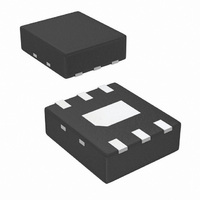
LP5900SD-3.0/NOPB National Semiconductor, LP5900SD-3.0/NOPB Datasheet - Page 9

LP5900SD-3.0/NOPB
Manufacturer Part Number
LP5900SD-3.0/NOPB
Description
IC REG LDO 150MA RF/ANLG 6-LLP
Manufacturer
National Semiconductor
Datasheet
1.LP5900SD-1.8EV.pdf
(12 pages)
Specifications of LP5900SD-3.0/NOPB
Regulator Topology
Positive Fixed
Voltage - Output
3V
Voltage - Input
Up to 5.5V
Voltage - Dropout (typical)
0.08V @ 150mA
Number Of Regulators
1
Current - Output
150mA (Max)
Operating Temperature
-40°C ~ 85°C
Mounting Type
Surface Mount
Package / Case
6-LLP
For Use With
LP5900SD-3.0EV - BOARD EVALUATION LP5900SD-3.0
Lead Free Status / RoHS Status
Lead free / RoHS Compliant
Current - Limit (min)
-
Other names
LP5900SD-3.0TR
Available stocks
Company
Part Number
Manufacturer
Quantity
Price
Part Number:
LP5900SD-3.0/NOPB
Manufacturer:
NS/国半
Quantity:
20 000
Also, tantalum capacitors can suffer catastrophic failures due
to surge current when connected to a low-impedance source
of power (like a battery or a very large capacitor). If a tantalum
capacitor is used at the input, it must be guaranteed by the
manufacturer to have a surge current rating sufficient for the
application. There are no requirements for the ESR (Equiva-
lent Series Resistance) on the input capacitor, but tolerance
and temperature coefficient must be considered when select-
ing the capacitor to ensure the capacitance will remain 0.47
μF ±30% over the entire operating temperature range.
OUTPUT CAPACITOR
The LP5900 is designed specifically to work with very small
ceramic output capacitors. A ceramic capacitor (dielectric
types X5R or X7R) in the 0.47 μF to 10 μF range, and with
ESR between 5 mΩ to 500 mΩ, is suitable in the LP5900 ap-
plication circuit. For this device the output capacitor should be
connected between the V
tion and should be mounted within 1 cm of the device.
It may also be possible to use tantalum or film capacitors at
the device output, V
reasons of size and cost (see the section Capacitor Charac-
teristics).
The output capacitor must meet the requirement for the min-
imum value of capacitance and have an ESR value that is
within the range 5 mΩ to 500 mΩ for stability.
CAPACITOR CHARACTERISTICS
The LP5900 is designed to work with ceramic capacitors on
the input and output to take advantage of the benefits they
offer. For capacitance values in the range of 0.47 μF to 4.7
μF, ceramic capacitors are the smallest, least expensive and
have the lowest ESR values, thus making them best for elim-
inating high frequency noise. The ESR of a typical 0.47 μF
ceramic capacitor is in the range of 20 mΩ to 40 mΩ, which
easily meets the ESR requirement for stability for the LP5900.
The temperature performance of ceramic capacitors varies by
type and manufacturer. Most large value ceramic capacitors
(
characteristics, which results in the capacitance dropping by
more than 50% as the temperature goes from 25°C to 85°C.
A better choice for temperature coefficient in a ceramic ca-
pacitor is X7R. This type of capacitor is the most stable and
holds the capacitance within ±15% over the temperature
range. Tantalum capacitors are less desirable than ceramic
for use as output capacitors because they are more expen-
sive when comparing equivalent capacitance and voltage
ratings in the 0.47 μF to 4.7 μF range.
Another important consideration is that tantalum capacitors
have higher ESR values than equivalent size ceramics. This
≥
2.2 µF) are manufactured with Z5U or Y5V temperature
OUT
, but these are not as attractive for
OUT
pin and a good ground connec-
9
means that while it may be possible to find a tantalum capac-
itor with an ESR value within the stable range, it would have
to be larger in capacitance (which means bigger and more
costly) than a ceramic capacitor with the same ESR value. It
should also be noted that the ESR of a typical tantalum will
increase about 2:1 as the temperature goes from 25°C down
to −40°C, so some guard band must be allowed.
NO-LOAD STABILITY
The LP5900 will remain stable and in regulation with no ex-
ternal load.
ENABLE CONTROL
The LP5900 may be switched ON or OFF by a logic input at
the ENABLE pin. A high voltage at this pin will turn the device
on. When the enable pin is low, the regulator output is off and
the device typically consumes 3nA. However if the application
does not require the shutdown feature, the V
to V
case the supply voltage must be fully established 500μs or
less to ensure correct operation of the start-up circuit. Failure
to comply with this condition may cause a delayed start-up
time of several seconds.
A 1MΩ pulldown resistor ties the V
sures that the device will remain off when the enable pin is
left open circuit. To ensure proper operation, the signal source
used to drive the V
below the specified turn-on/off voltage thresholds listed in the
Electrical Characteristics section under V
micro SMD MOUNTING
The micro SMD package requires specific mounting tech-
niques, which are detailed in National Semiconductor Appli-
cation Note AN-1112.
For best results during assembly, alignment ordinals on the
PC board may be used to facilitate placement of the micro
SMD device.
micro SMD LIGHT SENSITIVITY
Exposing the micro SMD device to direct light may cause in-
correct operation of the device. Light sources such as halogen
lamps can affect electrical performance if they are situated in
proximity to the device.
Light with wavelengths in the red and infra-red part of the
spectrum have the most detrimental effect thus the fluores-
cent lighting used inside most buildings has very little effect
on performance.
IN
to keep the regulator output permanently on. In this
EN
input must be able to swing above and
EN
input to ground, this en-
IL
and V
EN
pin can be tied
www.national.com
IH
.


