L4940V5 STMicroelectronics, L4940V5 Datasheet
L4940V5
Specifications of L4940V5
Available stocks


Related parts for L4940V5


L4940V5 Summary of contents
Page 1
... Table 1. Device summary Part numbers L4940XX5 L4940XX85 L4940XX10 L4940XX12 December 2009 L4940XX5, L4940XX85 L4940XX10, L4940XX12 Very low drop 1.5 A regulator Order codes TO-220 D²PAK L4940V5 L4940D2T5-TR L4940V85 L4940D2T10-TR L4940D2T12-TR Doc ID 2141 Rev 12 D²PAK TO-220 Output voltages www.st.com 1/23 ...
Page 2
Contents Contents 1 Block diagram . . . . . . . . . . . . . . . . . . . . . . . . . . . . . . . . . . . ...
Page 3
L4940XX5, L4940XX85, L4940XX10, L4940XX12 1 Block diagram Figure 1. Block diagram Doc ID 2141 Rev 12 Block diagram 3/23 ...
Page 4
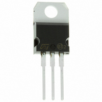
Pin configuration 2 Pin configuration Figure 2. Pin connections (top view) TO-220 4/23 L4940XX5, L4940XX85, L4940XX10, L4940XX12 D²PAK Doc ID 2141 Rev 12 TO-220FP ...
Page 5
L4940XX5, L4940XX85, L4940XX10, L4940XX12 3 Maximum ratings Table 2. Absolute maximum ratings Symbol V Forward input voltage I V Reverse input voltage IR I Output current O P Power dissipation D T Storage temperature range stg T Operating junction temperature ...
Page 6
Test circuits 4 Test circuits Figure 3. DC parameters Figure 4. Load rejection Figure 5. Ripple rejection 6/23 L4940XX5, L4940XX85, L4940XX10, L4940XX12 Doc ID 2141 Rev 12 ...
Page 7
L4940XX5, L4940XX85, L4940XX10, L4940XX12 5 Electrical characteristics Refer to test circuit, V Table 4. Electrical characteristics of L4940XX5 Symbol Parameter V Output voltage O V Output voltage O V Input voltage I ΔV Line regulation O ΔV Load regulation O ...
Page 8
Electrical characteristics Refer to test circuit, V specified. Table 5. Electrical characteristics of L4940XX85 Symbol Parameter V Output voltage O V Output voltage O V Input voltage I ΔV Line regulation O ΔV Load regulation O I Quiescent current q ...
Page 9
L4940XX5, L4940XX85, L4940XX10, L4940XX12 Refer to test circuit, V Table 6. Electrical characteristics of L4940XX10 Symbol Parameter V Output voltage O V Output voltage O V Input voltage I ΔV Line regulation O ΔV Load regulation O I Quiescent current ...
Page 10
Electrical characteristics Refer to test circuit, V Table 7. Electrical characteristics of L4940XX12 Symbol Parameter V Output voltage O V Output voltage O V Input voltage I ΔV Line regulation O ΔV Load regulation O I Quiescent current q ΔI ...
Page 11
... L4940XX5, L4940XX85, L4940XX10, L4940XX12 6 Typical application Figure 6. Dropout voltage vs. output current Figure 7. Figure 8. Output voltage vs. temperature (L4940V5) Figure 10. Output voltage vs. temperature (L4940V10) Dropout voltage vs. temperature Figure 9. Output voltage vs. temperature (L4940V85) Figure 11. Output voltage vs. temperature (L4940V12) Doc ID 2141 Rev 12 Typical application 11/23 ...
Page 12
... Figure 12. Quiescent current vs. temperature (L4940V5) Figure 14. Quiescent current vs. output current (L4940V5) Figure 16. Peak output current vs. input/output differential voltage (L4940V5) 12/23 L4940XX5, L4940XX85, L4940XX10, L4940XX12 Figure 13. Quiescent current vs. input voltage (L4940V5) Figure 15. Short circuit current vs. temperature (L4940V5) Figure 17. Low voltage behavior (L4940V5) Doc ID 2141 Rev 12 ...
Page 13
... L4940XX5, L4940XX85, L4940XX10, L4940XX12 Figure 18. Low voltage behavior (L4940V85) Figure 20. Low voltage behavior (L4940V12) Figure 22. Supply voltage rejection vs. output current (L4940V5) Figure 19. Low voltage behavior (L4940V10) Figure 21. Supply voltage rejection vs. frequency (L4940V5) Figure 23. Lad dump characteristics (L4940V5) Doc ID 2141 Rev 12 Typical application ...
Page 14
... Typical application Figure 24. Line transient response (L4940V5) Figure 26. Load transient response 14/23 L4940XX5, L4940XX85, L4940XX10, L4940XX12 Figure 25. Total power dissipation Doc ID 2141 Rev 12 ...
Page 15
L4940XX5, L4940XX85, L4940XX10, L4940XX12 7 Schematic application Figure 27. Distributed supply with on-card L4940 and L4941 low drop regulator Figure 28. Distributed supply with on-card L4940 and L4941 low drop regulator Note: Advantages of these application are: On card regulation ...
Page 16
Schematic application Figure 29. Distributed supply with on-card L4940 and L4941 low drop regulator Note: Advantages of this configuration are: Very high regulation (line and load on both the output voltage output short circuit and thermally protected. Very ...
Page 17
L4940XX5, L4940XX85, L4940XX10, L4940XX12 8 Package mechanical data In order to meet environmental requirements, ST offers these devices in different grades of ® ECOPACK packages, depending on their level of environmental compliance. ECOPACK specifications, grade definitions and product status are ...
Page 18
Package mechanical data Dim. Min. A 4.40 C 1. 0.49 F 0.61 F1 1.14 F2 1.14 G 4.95 G1 2 13.0 L5 2.65 L6 15.25 L7 6.2 L9 3.5 DIA. 3.75 18/23 ...
Page 19
L4940XX5, L4940XX85, L4940XX10, L4940XX12 Dim. Min. A 4.40 B 2.5 D 2.5 E 0.45 F 0.75 F1 1.15 F2 1.15 G 4.95 G1 2 28.6 L4 9.8 L5 2 DIA. 3 TO-220FP ...
Page 20
Package mechanical data Dim. Min. A 4.4 A1 2.49 A2 0.03 B 0.7 B2 1.14 C 0.45 C2 1. 1.27 L3 1 0° 20/23 L4940XX5, ...
Page 21
L4940XX5, L4940XX85, L4940XX10, L4940XX12 2 Tape & reel D PAK-P Dim. Min 12 10.50 Bo 15.70 Ko 4.80 Po 3 PAK-D PAK/A-P PAK/A mechanical data mm. Typ. ...
Page 22
Revision history 9 Revision history Table 8. Document revision history Date Revision 04-Feb-2005 6 18-Sep-2006 7 31-May-2007 8 19-Sep-2007 9 20-Feb-2008 10 29-Jul-2009 11 16-Dec-2009 12 22/23 L4940XX5, L4940XX85, L4940XX10, L4940XX12 Add new package D²PAK/A. Order codes has been updated ...
Page 23
... L4940XX5, L4940XX85, L4940XX10, L4940XX12 Information in this document is provided solely in connection with ST products. STMicroelectronics NV and its subsidiaries (“ST”) reserve the right to make changes, corrections, modifications or improvements, to this document, and the products and services described herein at any time, without notice. All ST products are sold pursuant to ST’s terms and conditions of sale. ...