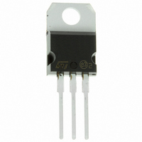
LD1117V50 STMicroelectronics, LD1117V50 Datasheet - Page 17

LD1117V50
Manufacturer Part Number
LD1117V50
Description
IC REG LDO POS 800MA 5V TO-220
Manufacturer
STMicroelectronics
Specifications of LD1117V50
Regulator Topology
Positive Fixed
Voltage - Output
5V
Voltage - Input
Up to 15V
Voltage - Dropout (typical)
1.1V @ 800mA
Number Of Regulators
1
Current - Output
950mA
Operating Temperature
0°C ~ 125°C
Mounting Type
Through Hole
Package / Case
TO-220-3 (Straight Leads)
Number Of Outputs
1
Polarity
Positive
Input Voltage Max
15 V
Output Voltage
5 V
Output Type
Fixed
Dropout Voltage (max)
1.1 V
Output Current
950 mA
Line Regulation
10 mV
Load Regulation
15 mV
Voltage Regulation Accuracy
1 %
Maximum Power Dissipation
12 W
Maximum Operating Temperature
+ 150 C
Mounting Style
Through Hole
Minimum Operating Temperature
0 C
Primary Input Voltage
7V
Output Voltage Fixed
5V
Dropout Voltage Vdo
1.1V
No. Of Pins
3
Voltage Regulator Case Style
TO-220
Operating Temperature Range
0°C To +125��C
Rohs Compliant
Yes
Lead Free Status / RoHS Status
Lead free / RoHS Compliant
Current - Limit (min)
-
Lead Free Status / Rohs Status
Lead free / RoHS Compliant
Other names
497-7311-5
LD1117V50
LD1117V50
Available stocks
Company
Part Number
Manufacturer
Quantity
Price
Company:
Part Number:
LD1117V50
Manufacturer:
ST
Quantity:
1 840
Company:
Part Number:
LD1117V50
Manufacturer:
STMicroelectronics
Quantity:
29 512
Company:
Part Number:
LD1117V50
Manufacturer:
XIL
Quantity:
7 082
Part Number:
LD1117V50
Manufacturer:
ST
Quantity:
20 000
Company:
Part Number:
LD1117V50C
Manufacturer:
SHARP
Quantity:
9 000
Figure 10: Post-Regulated Dual Supply
LD1117 ADJUSTABLE: APPLICATION NOTE
The LD1117 ADJUSTABLE has a thermal
stabilized 1.25±0.012V reference voltage between
the OUT and ADJ pins. I
max.) and ∆I
R1 is normally fixed to 120Ω. From figure 11 we
obtain:
V
+V
In normal application R2 value is in the range of
few kohm, so the R2 x I
considered in the V
above expression becomes:
OUT
REF
= V
/R1) = V
REF
ADJ
+ R2 (I
REF
is 1µA typ. (5µA max.).
(1 + R2 / R1) + R2 x I
ADJ
OUT
ADJ
DJ
+I
R1
calculation; then the
product could not be
is 60µA typ. (120µA
) = V
REF
+ R2 (I
ADJ
.
ADJ
V
In order to have the better load regulation it is
important to realize a good Kelvin connection of
R1 and R2 resistors. In particular R1 connection
must be realized very close to OUT and ADJ pin,
while R2 ground connection must be placed as
near as possible to the negative Load pin. Ripple
rejection can be improved by introducing a 10µF
electrolytic capacitor placed in parallel to the R2
resistor (see Fig. 12).
OUT
= V
REF
(1 + R2 / R1).
LD1117 SERIES
17/28


