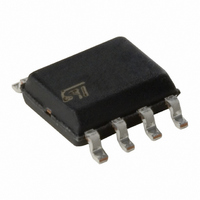
LK115D33-TR STMicroelectronics, LK115D33-TR Datasheet

LK115D33-TR
Specifications of LK115D33-TR
Available stocks
Related parts for LK115D33-TR
LK115D33-TR Summary of contents
Page 1
... Table 1. Device summary Order codes LK115D30-TR LK115D33-TR LK115D50-TR July 2008 LK115XX33 - LK115XX50 Very low drop with inhibit voltage regulators It requires only a 2.2 µF capacitor for stability allowing space and cost saving. ...
Page 2
Contents 1 Diagram . . . . . . . . . . . . . . . . . . . . . . . . . . . . . . . . . . . . . ...
Page 3
Diagram Figure 1. Schematic diagram 3/14 ...
Page 4
Pin configuration Figure 2. Pin connection (top view) Table 2. Truth table ON/OFF (Pin Note: Logic levels are those defined in the electrical characteristics. 4/14 ON/OFF (Pin Status ON ...
Page 5
Maximum ratings Table 3. Absolute maximum ratings Symbol V DC input voltage I I Output current O P Power dissipation TOT T Storage temperature range STG T Operating junction temperature range OP Note: Absolute maximum ratings are those values ...
Page 6
Test circuits Figure 3. Supply current (On mode) Figure 4. Supply current (Off mode) Note: The switch emulates the two possibilities to set the regulator in OFF mode. 6/14 ...
Page 7
Electrical characteristics Table 4. Electrical characteristics for LK115D30 (refer to the test circuits 2.2 µF unless otherwise specified.) O Symbol Parameter V Output voltage O V Operating input voltage I I Output current limit out ΔV ...
Page 8
... Table 5. Electrical characteristics for LK115D33 (refer to the test circuits 2.2 µF unless otherwise specified.) O Symbol Parameter V Output voltage O V Operating input voltage I I Output current limit out ΔV Line regulation O ΔV Load regulation O Quiescent current (On Mode (Off Mode) SVR Supply voltage rejection ...
Page 9
Table 6. Electrical characteristics for LK115D50 (refer to the test circuits 2.2 µF unless otherwise specified.) O Symbol Parameter V Output voltage O V Operating input voltage I I Output current limit out ΔV Line regulation O ...
Page 10
Package mechanical data In order to meet environmental requirements, ST offers these devices in ECOPACK packages. These packages have a lead-free second level interconnect. The category of second Level Interconnect is marked on the package and on the inner ...
Page 11
SO-8 mechanical data mm. Dim. Min. Typ. A 1.35 A1 0.10 A2 1.10 B 0.33 C 0.19 D 4.80 E 3.80 e 1.27 H 5.80 h 0.25 L 0.40 k ddd inch. Max. Min. Typ. 1.75 0.053 0.25 0.04 1.65 ...
Page 12
Tape & reel SO-8 mechanical data Dim. Min 12 8.1 Bo 5.5 Ko 2.1 Po 3.9 P 7.9 12/14 mm. Typ. Max. Min. 330 13.2 0.504 0.795 2.362 22.4 8.5 0.319 5.9 ...
Page 13
Revision history Table 7. Document revision history Date Revision 07-Jun-2006 3 07-Jul-2008 4 Changes Order codes updated. Added Table 1 on page 1. 13/14 ...
Page 14
... Information in this document is provided solely in connection with ST products. STMicroelectronics NV and its subsidiaries (“ST”) reserve the right to make changes, corrections, modifications or improvements, to this document, and the products and services described herein at any time, without notice. All ST products are sold pursuant to ST’s terms and conditions of sale. ...


