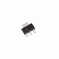
LD1117S25TR STMicroelectronics, LD1117S25TR Datasheet - Page 4

LD1117S25TR
Manufacturer Part Number
LD1117S25TR
Description
IC REG LDO POS 800MA 2.5V SOT223
Manufacturer
STMicroelectronics
Specifications of LD1117S25TR
Regulator Topology
Positive Fixed
Voltage - Output
2.5V
Voltage - Input
Up to 15V
Voltage - Dropout (typical)
1.1V @ 800mA
Number Of Regulators
1
Current - Output
950mA
Operating Temperature
0°C ~ 125°C
Mounting Type
Surface Mount
Package / Case
SOT-223 (3 leads + Tab), SC-73, TO-261
Number Of Outputs
1
Polarity
Positive
Input Voltage Max
15 V
Output Voltage
2.5 V
Output Type
Fixed
Dropout Voltage (max)
1.1 V
Output Current
950 mA
Line Regulation
6 mV
Load Regulation
10 mV
Voltage Regulation Accuracy
1 %
Maximum Power Dissipation
12 W
Maximum Operating Temperature
+ 150 C
Mounting Style
SMD/SMT
Minimum Operating Temperature
0 C
Primary Input Voltage
4.5V
Output Voltage Fixed
2.5V
Dropout Voltage Vdo
1.1V
No. Of Pins
3
Voltage Regulator Case Style
SOT-223
Operating Temperature Range
0°C To +125°C
Svhc
No
Rohs Compliant
Yes
Lead Free Status / RoHS Status
Lead free / RoHS Compliant
Current - Limit (min)
-
Lead Free Status / Rohs Status
Lead free / RoHS Compliant
Other names
497-7309-2
LD1117S25TR
LD1117S25TR
Available stocks
Company
Part Number
Manufacturer
Quantity
Price
Company:
Part Number:
LD1117S25TR
Manufacturer:
STMicroelectronics
Quantity:
32 558
Part Number:
LD1117S25TR
Manufacturer:
ST
Quantity:
20 000
LD1117 SERIES
Table 4: Electrical Characteristics Of LD1117#12 (refer to the test circuits, T
C
Table 5: Electrical Characteristics Of LD1117#18 (refer to the test circuits, T
C
4/27
Symbol
Symbol
O
O
I
O(min)
SVR
SVR
∆I
∆V
∆V
∆V
∆V
∆V
∆V
∆V
∆V
I
V
V
V
eN
V
V
V
eN
V
V
I
I
adj
= 10 µF, R = 120 Ω between GND and OUT pins, unless otherwise specified)
= 10 µF unless otherwise specified)
I
O
O
adj
d
in
in
O
O
O
O
d
d
O
O
O
O
O
O
O
O
Output Voltage
Reference Voltage
Line Regulation
Load Regulation
Temperature Stability
Long Term Stability
Operating Input Voltage
Adjustment Pin Current
Adjustment Pin Current
Change
Minimum Load Current
Output Current
Output Noise (%V
Supply Voltage Rejection
Dropout Voltage
Thermal Regulation
Output Voltage
Output Voltage
Line Regulation
Load Regulation
Temperature Stability
Long Term Stability
Operating Input Voltage
Quiescent Current
Output Current
Output Noise Voltage
Supply Voltage Rejection
Dropout Voltage
Thermal Regulation
Parameter
Parameter
O
)
V
I
V
V
1000 hrs, T
V
V
I
V
V
B =10Hz to 10KHz
I
V
I
I
I
T
V
I
V
V
1000 hrs, T
I
V
V
B =10Hz to 10KHz
I
V
I
I
I
T
O
O
O
O
O
O
O
O
O
O
O
O
a
a
in
in
in
in
in
in
in
in
in
in
in
in
in
in
= 10 to 800 mA
= 10 to 800 mA
= 40 mA f = 120Hz
= 100 mA
= 500 mA
= 800 mA
= 0 to 800 mA
= 100 mA
= 40 mA f = 120Hz
= 100 mA
= 500 mA
= 800 mA
= 25°C 30ms Pulse
= 25°C 30ms Pulse
= 3.2 V I
- V
- V
≤ 15 V
- V
= 15 V
- V
- V
= 3.8 V I
= 3.3 to 8 V
= 3.3 V
≤ 8 V
= 6.8 V T
= 5.5 V V
O
O
O
O
O
= 1.5 to 13.75 V
= 3 V
= 1.4 to 10 V
= 5 V
= 3 V
J
J
O
O
Test Conditions
Test Conditions
= 125°C
= 125°C
J
ripple
= 10 mA
= 10 mA
= 25°C
= 1 V
V
in
I
T
T
V
V
I
I
T
O
O
O
PP
J
J
J
ripple
in
- V
= 10 to 800 mA
= 0 mA
= 0 to 800 mA
= 25°C
= 25°C
= 25°C
= 3.3 to 8 V
O
= 1.4 to 10 V
= 1 V
T
I
T
T
T
O
J
J
J
J
= 10 mA
= 25°C
= 25°C
= 25°C
= 25°C
PP
1.188
1.140
Min.
Min.
1.78
1.76
800
800
60
60
J
J
= 0 to 125°C,
= 0 to 125°C,
0.035
0.003
Typ.
1.20
1.20
1.05
1.10
0.01
Typ.
1.05
1.10
0.01
950
950
100
0.1
0.5
0.3
1.8
0.5
0.3
60
75
75
1
2
1
1
1
5
1
1.212
1.260
Max.
1300
Max.
1300
1.15
1.82
1.84
1.15
120
0.2
0.4
1.1
1.2
0.1
1.1
1.2
0.1
15
10
10
10
5
5
6
%/W
%/W
Unit
Unit
mA
mA
mV
mV
mA
mA
µA
µA
dB
µV
dB
%
%
%
%
%
%
%
V
V
V
V
V
V
V
V


