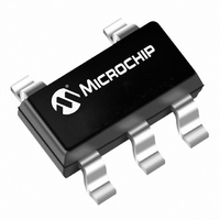
MCP1802T-5002I/OT Microchip Technology, MCP1802T-5002I/OT Datasheet - Page 3

MCP1802T-5002I/OT
Manufacturer Part Number
MCP1802T-5002I/OT
Description
IC REG LDO 300MA 5.0V SOT23-5
Manufacturer
Microchip Technology
Datasheet
1.MCP1802T-3302IOT.pdf
(28 pages)
Specifications of MCP1802T-5002I/OT
Package / Case
SOT-23-5, SC-74A, SOT-25
Regulator Topology
Positive Fixed
Voltage - Output
5V
Voltage - Input
Up to 10V
Voltage - Dropout (typical)
0.2V @ 100mA
Number Of Regulators
1
Current - Output
300mA (Min)
Operating Temperature
-40°C ~ 85°C
Mounting Type
Surface Mount
Number Of Outputs
1
Polarity
Positive
Input Voltage Max
10 V
Output Voltage
5 V
Output Type
Fixed
Dropout Voltage (max)
0.09 V at 30 mA
Output Current
300 mA
Line Regulation
0.2 % / V
Load Regulation
100 mV
Voltage Regulation Accuracy
2 %
Maximum Power Dissipation
0.25 W
Maximum Operating Temperature
+ 85 C
Mounting Style
SMD/SMT
Minimum Operating Temperature
- 40 C
Lead Free Status / RoHS Status
Lead free / RoHS Compliant
Current - Limit (min)
-
Lead Free Status / Rohs Status
Lead free / RoHS Compliant
Other names
MCP1802T-5002I/OT
MCP1802T-5002I/OTTR
MCP1802T-5002I/OTTR
Available stocks
Company
Part Number
Manufacturer
Quantity
Price
Part Number:
MCP1802T-5002I/OT
Manufacturer:
MICROCHIP/微芯
Quantity:
20 000
1.0
Absolute Maximum Ratings †
Input Voltage ................................................................. +12V
Output Current (Continuous) ..................... P
Output Current (Peak) ............................................... 500 mA
Output Voltage ............................... (V
SHDN Voltage ..................................(V
Continuous Power Dissipation:
ELECTRICAL CHARACTERISTICS
2010 Microchip Technology Inc.
Electrical Specifications: Unless otherwise specified, all limits are established for V
C
Input / Output Characteristics
Input Operating Voltage
Input Quiescent Current
Shutdown Current
Maximum Output Current
Current Limiter
Output Short Circuit Current
Output Voltage Regulation
V
Coefficient
Line Regulation
Load Regulation
Dropout Voltage,
Power Supply Ripple
Rejection Ratio
Output Noise
Note 1:
5-Pin SOT-23-5 .................................................... 250 mW
OUT
IN
= 1 µF (X7R), V
Temperature
2:
3:
4:
5:
Parameters
ELECTRICAL
CHARACTERISTICS
The minimum V
V
The input voltage V
TCV
temperature range. V
Load regulation is measured at a constant junction temperature using low duty cycle pulse testing. Changes in output
voltage due to heating effects are determined using thermal regulation specification TCV
Dropout voltage is defined as the input to output differential at which the output voltage drops 2% below its measured
value with an applied input voltage of V
R
is the nominal regulator output voltage. For example: V
OUT
Note 5
SHDN
= (V
OUT-HIGH
= V
IN
IN
(V
must meet two conditions: V
, T
V
V
IN
TCV
OUT
I
I
V
DROPOUT
OUT_mA
OUT_SC
OUT
A
PSRR
OUT-LOW
I
I
V
= V
Sym
SHDN
LIMIT
V
- V
= +25°C
e
OUT
I
OUT
XV
IN
q
N
OUT
/V
R
SS
SS
OUT-LOW
OUT
/
+ 1.0V or Vi
-0.3V) to (V
-0.3V) to (V
IN
)
= lowest voltage measured over the temperature range.
D
V
/(V
V
) *10
R
R
-30 mV
IN
Min
300
300
260
260
-0.2
2.0
-2.0%
—
—
—
—
—
—
—
—
—
—
—
—
—
—
—
-V
6
IN
R
IN
IN
OUT
/ (V
+ 1.0V or 2.0V, whichever is greater.
+0.3V)
+0.3V)
= 2.0V (whichever is greater); I
)mA
R
2.07 - V
2.23 - V
* Temperature), V
IN
±0.01
0.01
0.46
Typ
380
100
200
240
V
V
2.0V and V
25
50
15
60
80
70
—
—
—
—
—
—
R
R
R
R
V
V
2.10 - V
2.33 - V
R
† Notice: Stresses above those listed under “Maximum
Ratings” may cause permanent damage to the device.
This is a stress rating only and functional operation of
the device at those or any other conditions above those
indicated in the operational listings of this specification
is not implied. Exposure to maximum rating conditions
for extended periods may affect device reliability.
R
R
+30 mV
Max
10.0
0.10
+0.2
+2.0%
100
250
120
350
= 1.8V, 2.5V, 3.0V, 3.3V, or 5.0V.
50
50
90
—
—
—
—
—
—
—
—
—
IN
(V
R
R
OUT-HIGH
R
ppm/°C
μV/√Hz
+ 1.0V).
Units
%/V
OUT
IN
mA
mA
mA
mV
mV
µA
µA
dB
V
V
V
= highest voltage measured over the
= V
= 100 µA.
R
+ 1.0V,
Note 1
I
SHDN = 0V
V
1.5V V
1.0V V
0.9V V
if V
if V
V
V
I
Note 3
(V
V
V
I
I
I
I
I
I
I
I
f = 10 kHz, I
pk-pk, C
if V
1 μF (X7R Ceramic), V
L
OUT
L
L
L
L
L
L
L
L
I
OUT
R
R
R
R
R
= 0 mA
R
= 1.0 mA to 100 mA,
= 1.0 mA to 300 mA,
= 30 mA, 3.1V V
= 100 mA, 3.1V V
= 30 mA, 2.0V V
= 100 mA, 2.0V V
= 30 mA,V
= 100 mA, V
R
R
R
2V, V
1.45V, I
1.45V, I
1.75V, I
1.75V, I
+ 1V) V
1.75V, then V
1.75V, then V
= 30 mA, -40°C T
1.5V, then V
= 100 mA, f = 1 kHz, C
Note
OUT
IN
R
R
R
MCP1802
.
IN
= 0 µF,
2.0V, V
1.5V, V
1.0V, V
1, C
L
Conditions
OUT
OUT
OUT
OUT
= V
R
= 50 mA, V
IN
R
2.0V
OUT
R
< 2.0V
= 30 mA,
= 30 mA
10V,
= 30 mA
= 10 mA
+1.0V
DS22053C-page 3
IN
IN
IN
IN
= 1 µF (X7R),
IN
IN
R
R
= 2.5V
=3.0V
=2.5V
R
R
= V
= V
= V
OUT
6.0V
3.1V
Note 4
Note 1
A
6.0V
< 3.1V
INAC
R
+85°C,
R
R
Note 2
= 2.5V
+1.5V
+ 2.0V
+ 2.0V
OUT
= 1V
=


