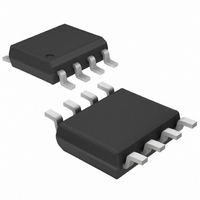
MAX817LCSA+T Maxim Integrated Products, MAX817LCSA+T Datasheet - Page 14

MAX817LCSA+T
Manufacturer Part Number
MAX817LCSA+T
Description
IC SUPERVISOR MPU 5V 8-SOIC
Manufacturer
Maxim Integrated Products
Type
Battery Backup Circuitr
Datasheet
1.MAX819LCSA.pdf
(16 pages)
Specifications of MAX817LCSA+T
Number Of Voltages Monitored
1
Reset
Active Low
Reset Timeout
140 ms Minimum
Voltage - Threshold
4.65V
Operating Temperature
0°C ~ 70°C
Mounting Type
Surface Mount
Package / Case
8-SOIC (3.9mm Width)
Lead Free Status / RoHS Status
Lead free / RoHS Compliant
Output
-
+5V Microprocessor Supervisory Circuits
desired trip point (V
It will typically be an order of magnitude greater than R1
or R2. The current through R1 and R2 should be at least
1µA to ensure that the 25nA (max) PFI input leakage
current does not shift the trip point. R3 should be larger
than 200k to prevent it from loading down the PFO pin.
Capacitor C1 adds additional noise rejection.
The MAX817/MAX819 µP supervisors can monitor either
positive or negative supplies using a resistor voltage
divider to PFI. PFO can be used to generate an interrupt
to the µP or to trigger a reset (Figures 9 and 13).
µPs with bidirectional reset pins, such as the Motorola
68HC11 series, can contend with the MAX817/MAX818/
MAX819 RESET output. If, for example, the RESET out-
put is driven high and the µP wants to pull it low, inde-
terminate logic levels may result. To correct this,
connect a 4.7k
and the µP reset I/O, as in Figure 14. Buffer the RESET
output to other system components.
These supervisors are relatively immune to short-dura-
tion, negative-going V
issuing a reset to the µP during power-up, power-down,
and brownout conditions. Therefore, resetting the µP
when V
desirable.
The Typical Operating Characteristics show a graph of
Maximum Transient Duration vs. Reset Threshold
Overdrive for which reset pulses are not generated. The
graph was produced using negative-going V
starting at 3.3V and ending below the reset threshold by
the magnitude indicated (reset threshold overdrive). The
graph shows the maximum pulse width that a negative-
going V
a reset pulse. As the amplitude of the transient increases
(i.e., goes farther below the reset threshold), the maxi-
mum allowable pulse width decreases. Typically, a V
transient that goes 100mV below the reset threshold and
lasts for 135µs will not trigger a reset pulse.
A 0.1µF bypass capacitor mounted close to the V
pin provides additional transient immunity.
14
______________________________________________________________________________________
CC
CC
experiences only small glitches is usually not
transient can typically have without triggering
Monitoring an Additional Supply
Negative-Going V
resistor between the RESET output
TRIP
CC
). Resistor R3 adds hysteresis.
Bidirectional Reset Pins
Interfacing to µPs with
transients (glitches) while
(MAX817/MAX819)
CC
Transients
CC
pulses,
CC
CC
Figure 13. Monitoring a Negative Voltage
Figure 14. Interfacing to µPs with Bidirectional Reset I/O
PFO
NOTE: V
5
+5V
+5V
0V
- 1.25
R1
MAX817
MAX818
MAX819
GND
V
R
R
CC
TRIP
1
2
=
V-
RESET
IS NEGATIVE
1.25 - V
R2
TRIP
BUFFERED RESET TO OTHER SYSTEM COMPONENTS
4.7k
PFI
V
TRIP
V-
MAX817
MAX819
GND
V
CC
RESET
GND
V
PFO
CC
0V


