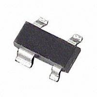
ADM6315-26D4ART-RL Analog Devices Inc, ADM6315-26D4ART-RL Datasheet - Page 7

ADM6315-26D4ART-RL
Manufacturer Part Number
ADM6315-26D4ART-RL
Description
IC SUPERVISOR OD 2.63V SOT143
Manufacturer
Analog Devices Inc
Type
Simple Reset/Power-On Resetr
Datasheet
1.ADM6315-44D3ARTZRL.pdf
(12 pages)
Specifications of ADM6315-26D4ART-RL
Rohs Status
RoHS non-compliant
Number Of Voltages Monitored
1
Output
Open Drain or Open Collector
Reset
Active Low
Reset Timeout
1.12 s Minimum
Voltage - Threshold
2.63V
Operating Temperature
-40°C ~ 125°C
Mounting Type
Surface Mount
Package / Case
SOT-143, SOT-143B, TO-253AA
Other names
ADM6315-26D4ARTRL
THEORY OF OPERATION
INTERFACING TO OUTPUT OF OTHER DEVICES
The ADM6315 series is designed to integrate with as many devices
as possible. One feature of the ADM6315 is the RESET open-
drain output, which can sink current from sources with a
voltage greater than the V
suitable for use in more diverse applications.
BENEFITS OF A VERY ACCURATE RESET THRESHOLD
Because the ADM6315 series can operate effectively even when
there are large degradations of the supply voltages (due to an
accurate internal voltage reference circuit), the possibility of a
malfunction during a power failure is greatly reduced.
DETAILED DESCRIPTION
The ADM6315 is designed to protect the integrity of a system’s
operation by ensuring the proper operation of the system
during power-up, power-down, and brownout conditions.
When the ADM6315 is powered up, the
ADM6315 remains low for a period typically equal to the RESET
active timeout period. This feature allows adequate time for the
system to power up correctly and for the power supply to
stabilize before any devices are brought out of reset and allowed
to begin executing instructions. Initializing a system in this way
provides a more reliable startup for microprocessor systems.
When a brownout condition occurs (assuming V
1 mV/μs), the ADM6315 produces a reset in 35 μs typical.
Producing a reset this fast means that the entire system can be
reset together before any part of the system’s voltage falls below
its recommended operating voltage. This system reset can avoid
dangerous and/or erroneous operation of a microprocessor-
based system.
Figure 10. V
V
RESET
CC
V
CC
TRIP POINT (MAX)
V
V
CC
CC
CC
Power-Down/Brownout Timing Diagram
TO RESET
TRIP POINT
DELAY
CC
of the ADM6315 input, making it
V
CC
VOL
TRIP POINT (MIN)
RESET
output of the
CC
is falling at
Rev. E | Page 7 of 12
MANUAL RESET INPUT
The ADM6315 also provides an additional input, MR . This
input can be used either as a means for the system operator to
reset the system manually via a switch or for a digital circuit to
reset the system.
The
faster than 100 ns, and it is guaranteed to accept any negative-
going input pulse of a duration greater than or equal to 1 μs. If
MR is connected to long cables or is used in a noisy environment,
placing a 1 μF decoupling capacitor between the MR input and
ground further improves the glitch immunity of the ADM6315.
TRANSIENT IMMUNITY
As well as being an accurate reset circuit, the ADM6315 has
good immunity from negative-going transients (see Figure 7).
Because of this characteristic, the ADM6315 is suitable for use
in noisy environments.
Figure 7 shows the
magnitude of negative-going pulses with respect to the typical
reset threshold) vs. the pulse duration without a reset.
V
CC
MR
TRIP POINT (MIN)
input (typically) ignores negative-going pulses that are
RESET
V
CC
Figure 11. V
RESET
CC
V
CC
Power-Up Timing Diagram
RESET ACTIVE TIMEOUT
comparator overdrive (the maximum
V
TRIP POINT
CC
TRIP POINT (MAX)
ADM6315


