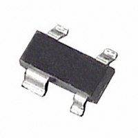
ADM6315-26D4ART-RL Analog Devices Inc, ADM6315-26D4ART-RL Datasheet

ADM6315-26D4ART-RL
Specifications of ADM6315-26D4ART-RL
Related parts for ADM6315-26D4ART-RL
ADM6315-26D4ART-RL Summary of contents
Page 1
... GND Figure 2. Typical Operating Circuit The manual reset function is very useful, especially if the circuit in which the ADM6315 is operating enters into a state that can be detected only by the user. Allowing the user to reset a system manually can reduce the damage or danger that could otherwise be caused by an out-of-control or locked-up system ...
Page 2
... ADM6315 TABLE OF CONTENTS Features .............................................................................................. 1 Applications....................................................................................... 1 Functional Block Diagram .............................................................. 1 General Description ......................................................................... 1 Revision History ............................................................................... 2 Specifications..................................................................................... 3 Absolute Maximum Ratings............................................................ 4 Thermal Resistance ...................................................................... 4 ESD Caution.................................................................................. 4 Pin Configuration and Function Descriptions............................. 5 REVISION HISTORY 9/07—Rev Rev. E Changes to Absolute Maximum Ratings ....................................... 4 Updated Outline Dimensions ......................................................... 8 Changes to Ordering Guide ............................................................ 8 4/06—Rev Rev. D Updated Format ...
Page 3
... −40°C to +125° −40°C to +85° −40°C to +125° −40°C to +85° −40°C to +125° > > < < μ kΩ > SINK V V > SINK V V > μA CC SINK μA V > RESET deasserted CC TH ADM6315 ...
Page 4
... ADM6315 ABSOLUTE MAXIMUM RATINGS T = 25°C, unless otherwise noted. A Table 2. Parameter Terminal Voltage (with Respect to Ground All Other Inputs Input Current V CC Output Current RESET Operating Temperature Range Storage Temperature Range Lead Temperature (Soldering, 10 sec) Vapor Phase (60 sec) Infrared (15 sec) ESD Rating Stresses above those listed under Absolute Maximum Ratings may cause permanent damage to the device ...
Page 5
... Manual Reset. This active low debounced input ignores input pulses of 100 ns (typical) and is guaranteed to accept input pulses of greater than 1 μs. Leave floating when not used Monitored Supply Voltage GND ADM6315 TOP VIEW (Not to Scale RESET MR Figure 3. Pin Configuration is below the reset threshold or when MR is low. RESET CC Rev Page ADM6315 rises above the reset threshold CC ...
Page 6
... ADM6315 TYPICAL PERFORMANCE CHARACTERISTICS 5. –40 – TEMPERATURE (°C) Figure 4. Supply Current vs. Temperature 450 400 350 300 250 200 V OD 150 100 V = 125mV 200mV OD 0 –40 – TEMPERATURE (°C) Figure 5. Power-Down Reset Delay vs. Temperature 1.06 1.04 1.02 1.00 0.98 0.96 0.94 –40 – ...
Page 7
... THEORY OF OPERATION INTERFACING TO OUTPUT OF OTHER DEVICES The ADM6315 series is designed to integrate with as many devices as possible. One feature of the ADM6315 is the RESET open- drain output, which can sink current from sources with a voltage greater than the V of the ADM6315 input, making it CC suitable for use in more diverse applications ...
Page 8
... ADM6315-26D1ARTRL7 −40°C to +125°C ADM6315-26D1ART-RL −40°C to +125°C 1 ADM6315-26D1ARTZR7 −40°C to +125°C 1 −40°C to +125°C ADM6315-26D1ARTZRL ADM6315-46D2ARTRL7 −40°C to +125°C ADM6315-46D2ART-RL −40°C to +125°C 1 −40°C to +125°C ADM6315-46D2ARTZR7 ADM6315-45D2ARTRL7 −40°C to +125°C ADM6315-45D2ART-RL – ...
Page 9
... ADM6315-29D4ARTRL7 −40°C to +125°C ADM6315-29D4ART-RL −40°C to +125°C 1 −40°C to +125°C ADM6315-29D4ARTZR7 ADM6315-26D4ARTRL7 −40°C to +125°C ADM6315-26D4ART-RL –40°C to +125°C 1 ADM6315-26D4ARTZR7 −40°C to +125°C 1 –40°C to +125°C ADM6315-26D4ARTZRL RoHS-Compliant Part, # denotes lead-free product may be top or bottom marked. ...
Page 10
... ADM6315 NOTES Rev Page ...
Page 11
... NOTES Rev Page ADM6315 ...
Page 12
... ADM6315 NOTES ©1999–2007 Analog Devices, Inc. All rights reserved. Trademarks and registered trademarks are the property of their respective owners. D00081-0-9/07(E) Rev Page ...


