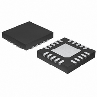
MAX6791TPLD2+T Maxim Integrated Products, MAX6791TPLD2+T Datasheet - Page 16

MAX6791TPLD2+T
Manufacturer Part Number
MAX6791TPLD2+T
Description
IC REG LINEAR DUAL 20-TQFN
Manufacturer
Maxim Integrated Products
Type
Regulator/Supervisorr
Datasheet
1.MAX6796TPLD2T.pdf
(25 pages)
Specifications of MAX6791TPLD2+T
Number Of Voltages Monitored
1
Output
Open Drain or Open Collector
Reset
Active Low
Reset Timeout
8.75 ms Minimum
Voltage - Threshold
4.625V
Operating Temperature
-40°C ~ 125°C
Mounting Type
Surface Mount
Package / Case
20-TQFN Exposed Pad
Number Of Outputs
2
Polarity
Positive
Input Voltage Max
72 V
Output Voltage
1.8 V to 11 V, 5 V
Output Type
Adjustable, Fixed
Dropout Voltage (max)
1.8 V at 150 mA
Output Current
150 mA
Line Regulation
1 %
Load Regulation
1.5 %
Maximum Power Dissipation
2.6667 W
Maximum Operating Temperature
+ 125 C
Mounting Style
SMD/SMT
Minimum Operating Temperature
- 40 C
Lead Free Status / RoHS Status
Lead free / RoHS Compliant
Other names
MAX6791TPLD2+TTR
The MAX6791–MAX6796 include a watchdog timer
that asserts RESET if the watchdog input (WDI) does
not toggle high to low or low to high within the watch-
dog timeout period t
adjustable). RESET remains low for the fixed or user-
adjustable reset timeout period, t
not updated for lengthy periods of time, the reset out-
put appears as a pulse train, asserted for t
deasserted for t
RESET asserts, it stays low for the entire reset timeout
period ignoring any WDI transitions that may occur. To
prevent the watchdog from asserting RESET, toggle
WDI with a valid rising or falling edge before t
the last edge. The watchdog counter clears when WDI
toggles prior to t
asserts. The watchdog resumes counting after RESET
deasserts.
The MAX6791/MAX6792 have a windowed watchdog
timer that asserts RESET for the adjusted reset timeout
period when the watchdog recognizes a fast watchdog
fault (t
t
dently of the watchdog timeout period.
The MAX6791–MAX6796 support two logic inputs,
ENABLE1/ENABLE and HOLD, making these devices
suitable for automotive applications. For example, when
the ignition key signal drives ENABLE1/ENABLE high,
the regulator turns on and remains on even if
ENABLE1/ENABLE goes low, as long as HOLD is forced
low and stays low after initial regulator power-up. In this
state, releasing HOLD turns the regulator output
(OUT/OUT1) off. This feature makes it possible to imple-
ment a self-holding circuit without external components.
Forcing ENABLE1/ENABLE low and HOLD high or
unconnected places the MAX6791–MAX6796 into shut-
down mode in which the MAX6791–MAX6796 draw less
than 27µA of supply current.
Table 3 shows the state of the regulator output with
respect to the voltage level at ENABLE1/ENABLE and
HOLD. Connect HOLD to OUT1/OUT or leave it uncon-
nected to allow the ENABLE1/ENABLE input to act as a
standard ON/OFF switch for the regulator output
(OUT/OUT1).
PFI is the noninverting input to a comparator. If PFI is
less than V
for the power-fail comparator include monitoring the
High-Voltage, Micropower, Single/Dual Linear
Regulators with Supervisory Functions
16
WD2
). The reset timeout period is adjusted indepen-
______________________________________________________________________________________
WDI
< t
PFI
WD1
(1.231V), PFO goes low. Common uses
WD
WD
), or a slow watchdog fault (t
, until WDI is toggled again. Once
from the last edge or when RESET
WD
Enable and Hold Inputs
Power-Fail Comparator
(280ms min or externally
RP
Watchdog Timer
. If the watchdog is
WD
WDI
from
RP
>
,
preregulated input of the power supply (such as a bat-
tery) or providing an early power-fail warning so soft-
ware can conduct an orderly system shutdown. Set the
power-fail threshold with a resistive-divider, as shown in
Figure 5. The typical comparator delay is 35µs from PFI
to PFO. Connect PFI to GND or IN if unused.
The MAX6791–MAX6796 include an overvoltage pro-
tection circuit that is capable of driving a p-channel
MOSFET to protect against reverse-battery conditions.
This MOSFET eliminates the need for external diodes,
thus minimizing the input voltage drop. See the Typical
Application Circuit. The low p-channel MOSFET on-
resistance of 30mΩ or less yields a forward-voltage
drop of only a few millivolts versus hundreds of milli-
volts for a diode, thus improving efficiency in battery-
operated devices. Connecting a positive battery
voltage to the drain of Q1 (see the Typical Application
Circuit) forward biases its body diode. When the source
voltage exceeds Q1’s threshold voltage, Q1 turns on.
Once the FET is on, the battery is fully connected to the
system and can deliver power to the device and the
load. An incorrectly inserted battery reverse-biases the
FET’s body diode. The gate remains at the ground
potential. The FET remains off and disconnects the
reversed battery from the system. The internal zener
diode and resistor combination at GATEP prevent dam-
age to the p-channel MOSFET during an overvoltage
condition. See the Functional Diagrams.
When the junction temperature exceeds T
the internal protection circuit turns off the internal pass
transistor and allows the IC to cool. The thermal sensor
turns the pass transistor on again after the junction tem-
perature drops to +145°C, resulting in a cycled output
during continuous thermal-overload conditions.
Thermal protection protects the MAX6791–MAX6796 in
the event of fault conditions. For continuous operation,
do not exceed the absolute maximum junction temper-
ature rating of +150°C.
The MAX6791–MAX6796 package features an exposed
thermal pad on its underside that should be used as a
heatsink. This pad lowers the package’s thermal resis-
tance by providing a direct heat-conduction path from
the die to the PC board. Connect the exposed pad and
GND to the system ground using a large pad or ground
plane, or multiple vias to the ground plane layer.
Proper Soldering of Package Heatsink
Reverse-Battery Protection Circuitry
Thermal Protection
J
= +165°C,


