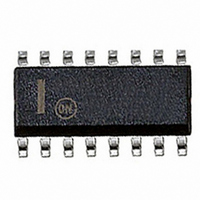
NE5517D ON Semiconductor, NE5517D Datasheet - Page 7

NE5517D
Manufacturer Part Number
NE5517D
Description
IC AMP XCONDUCTANCE DUAL 16-SOIC
Manufacturer
ON Semiconductor
Datasheet
1.NE5517DG.pdf
(14 pages)
Specifications of NE5517D
Amplifier Type
Transconductance
Number Of Circuits
2
Output Type
Push-Pull
Slew Rate
50 V/µs
Gain Bandwidth Product
2MHz
Current - Input Bias
400nA
Voltage - Input Offset
400µV
Current - Supply
2.6mA
Current - Output / Channel
650µA
Voltage - Supply, Single/dual (±)
4 V ~ 44 V, ±2 V ~ 22 V
Operating Temperature
0°C ~ 70°C
Mounting Type
Surface Mount
Package / Case
16-SOIC (3.9mm Width)
Number Of Channels
2
Input Offset Voltage
5 mV
Supply Voltage (max)
44 V
Supply Current
4 mA
Maximum Operating Temperature
+ 70 C
Minimum Operating Temperature
0 C
Common Mode Rejection Ratio (min)
80 dB
Input Voltage Range (max)
Positive Rail - 3 V
Maximum Power Dissipation
1125 mW
Mounting Style
SMD/SMT
Lead Free Status / RoHS Status
Contains lead / RoHS non-compliant
-3db Bandwidth
-
Lead Free Status / Rohs Status
Details
Available stocks
Company
Part Number
Manufacturer
Quantity
Price
Part Number:
NE5517D
Manufacturer:
NXP/恩智浦
Quantity:
20 000
AU5517/NE5517, a dual operational transconductance
amplifier with linearizing diodes and impedance buffers, is
shown in Figure 21.
Transconductance Amplifier
stage. The ratio of their collector currents (I
respectively) is defined by the differential input voltage, V
which is shown in Equation 1.
Where V
focuses the sum of current I
current I
The circuit schematic diagram of one-half of the
The transistor pair, Q
KT ≅ 26 mV at room temperature (300°k).
Transistors Q
B
IN
:
AMP BIAS
INPUT
−INPUT
is the difference of the two input voltages
V+
V−
2,15
11
1
6
CIRCUIT DESCRIPTION
, Q
4,13
1,16
2
D2
and diode D
INPUT
Q1
V
IN
4
I
4
and Q
) I
4
Q6
D1
+
Q4
and I
5
KT
Q2
q In
+ I
5
1
5
51W
, forms a transconductance
Q7
form a current mirror which
to be equal to amplifier bias
Q5
10kW
B
D4
I
I
5
4
D3
1.3kW
Figure 21. Circuit Diagram of NE5517
390pF
+INPUT
3,14
NE5517, NE5517A, AU5517
Figure 20. Unity Gain Follower
4
3, 14
2, 15
4, 13
and I
Q10
(eq. 2)
http://onsemi.com
Q8
APPLICATIONS
(eq. 1)
IN
−
+
5
,
,
10kW
NE5517
7
Q9
Q11
−15V
the Taylor series of In function can be approximated as
The remaining transistors (Q
form three current mirrors that produce an output current equal
to I
The term
and is proportional to I
D6
D5
11
6
0.001mF
+15V
If V
0.01mF
V OUTPUT
5
5,12
1, 16
minus I
IN
KT
is small, the ratio of I
q In
5, 12
62kW
2KT
I
B
7, 10
4
q
. Thus:
Q15
I
I
5
4
is then the transconductance of the amplifier
R1
[ KT q
Q14
KT
V
q In
Q16
0.01mF
I
IN
and I
5
* I
I
B
1 2I
5
I
.
* I
B
−15V
I
I
5kW
5
4
4
8, 9
2KT
4
[ KT q
+ V
B
q
7,10
D7
D8
6
4
^ I
OUTPUT
5
+ 2KT
to Q
and I
IN
5
+ I
Q12
^ I
I
q
11
2KT
5
4
I
B
) and diodes (D
Q3
* I
will approach unity and
I
q
O
B
I
4
5
* I
Q13
I
4
B
8,9
4
+ V
IN
4
(eq. 3)
(eq. 4)
(eq. 5)
to D
6
)


