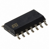
TS652ID STMicroelectronics, TS652ID Datasheet

TS652ID
Specifications of TS652ID
Available stocks
Related parts for TS652ID
TS652ID Summary of contents
Page 1
... APPLICATION Preamplifier and automatic gain control for Assymetric Digital Subscriber Line (ADSL). ORDER CODE Part Number Temperature Range TS652ID -40, +85° Small Outline Package (SO) - also available in Tape & Reel (DT) October 2001 (Plastic Micropackage) PIN CONNECTIONS (top view) +Vcc1 ...
Page 2
... TS652 ABSOLUTE MAXIMUM RATINGS Symbol V 1) Supply voltage Input Voltage i T Operating Free Air Temperature Range TS652ID oper T Storage Temperature std T Maximum Junction Temperature j R Thermal Resistance Junction to Case thjc R Thermal Resistance Junction to Ambiante Area thja Output Short Circuit Duration 1. All voltages values are with respect to network terminal. ...
Page 3
ELECTRICAL CHARACTERISTICS. V Symbol Parameter DC PERFORMANCE V Voltage on the Input Pin i I Total Supply Current CC V Differential Input Offset Voltage OFFSET SVR Supply Voltage Rejection Ratio POWER DOWN MODE Thershold Voltage for Power V pdw Down ...
Page 4
TS652 DIGITAL INPUTS Symbol Parameter Low Level GC1, GC2, GC3 and GC4 High Level SIMPLIFIED SCHEMATIC The TS652 consists of two independent channels. Each channel has two stages. The first is a very low noise digitally controlled variable gain amplifier ...
Page 5
BANDWIDTH The small signal bandwidth is almost constant for gains between +18dB to 0dB and is in the order of 52MHz to 70MHz respectively. For 30dB gain the bandwidth is around 18MHz. The power bandwidth is typically equal to 30MHz ...
Page 6
TS652 GAIN CONTROL The gain and the power down mode is programmed with a 4 bit digital word : Digital First Stage Control Total Gain (dB) GC4....GC1 MSB LSB $0000 -9 $0001 -6 $0010 -3 $0011 0 $0100 3 $0101 ...
Page 7
Closed Loop Gain vs Frequency -10 -20 -30 -40 10kHz 100kHz 1MHz 10MHz Frequency Negative & Positive Slew Rate vs Gain 110 105 SR- 100 95 SR ...
Page 8
TS652 Output/Input Isolation in Power Down Mode vs Frequency -50 -60 -70 -80 -90 -100 -110 10kHz 100kHz Frequency measurement conditions: Vcc= 6V, Rload=500 8/9 3rd Order Intermodulation (2 tones : 180kHz and 280kHz) -70 -75 -80 380kHZ -85 640kHZ ...
Page 9
... No license is granted by implication or otherwise under any patent or patent rights of STMicroelectronics. Specifications mentioned in this publication are subject to change without notice. This publication supersedes and replaces all information previously supplied ...


