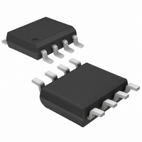
MAX410BESA Maxim Integrated Products, MAX410BESA Datasheet - Page 8

MAX410BESA
Manufacturer Part Number
MAX410BESA
Description
IC OPAMP LN LV PREC 28MHZ 8-SOIC
Manufacturer
Maxim Integrated Products
Datasheet
1.MAX410CSA.pdf
(13 pages)
Specifications of MAX410BESA
Amplifier Type
General Purpose
Number Of Circuits
1
Slew Rate
4.5 V/µs
Gain Bandwidth Product
28MHz
Current - Input Bias
80nA
Voltage - Input Offset
120µV
Current - Supply
2.5mA
Current - Output / Channel
35mA
Voltage - Supply, Single/dual (±)
4.8 V ~ 10.5 V, ±2.4 V ~ 5.25 V
Operating Temperature
-40°C ~ 85°C
Mounting Type
Surface Mount
Package / Case
8-SOIC (3.9mm Width)
Lead Free Status / RoHS Status
Contains lead / RoHS non-compliant
Output Type
-
-3db Bandwidth
-
Single/Dual/Quad, 28MHz, Low-Noise,
Low-Voltage, Precision Op Amps
The MAX410/MAX412/MAX414 provide low voltage-
noise performance. Obtaining low voltage noise from a
bipolar op amp requires high collector currents in the
input stage, since voltage noise is inversely proportion-
al to the square root of the input stage collector current.
However, op amp current noise is proportional to the
square root of the input stage collector current, and the
input bias current is proportional to the input stage col-
lector current. Therefore, to obtain optimum low-noise
performance, DC accuracy, and AC stability, minimize
the value of the feedback and source resistance.
The standard expression for the total input-referred
noise of an op amp at a given frequency is:
where:
R
R
e
interest
i
interest
T = Ambient temperature in Kelvin (K)
k = 1.28 x 10
In Figure 1, R
cation, the output resistance of the source driving the
input must be included with R
example demonstrates how to calculate the total out-
put-noise density at a frequency of 1kHz for the
MAX412 circuit in Figure 1.
Gain = 1000
4kT at +25°C = 1.64 x 10
R
R
e
i
e
x 10
Output noise density = (100)e
In general, the amplifier’s voltage noise dominates with
equivalent source resistances less than 200Ω. As the
equivalent source resistance increases, resistor noise
8
n
Total Noise Density vs. Source Resistance
n
n
n
t
n
p
p
n
= 1.2pA/√Hz at 1kHz
= [(1.5 x 10
= Input current-noise density at the frequency of
= 1.5nV/√Hz at 1kHz
= Inverting input effective series resistance
= Noninverting input effective series resistance
= 100Ω || 100kΩ = 99.9 W
= Input voltage-noise density at the frequency of
= 100Ω
_______________________________________________________________________________________
-20
) (100 + 99.9)]
e
t
=
-23
e
p
-9
n
= R3 and R
)
Applications Information
2
J/K (Boltzman’s constant)
2
+(R +R )
+ (100 + 99.9)
p
1/2
= 2.36nV/√Hz at 1kHz
-20
n
n
2
= R1 || R2. In a real appli-
i
t
n
= 2.36µV/√Hz at 1kHz.
2
p
+ 4kT (R +R )
2
and R
(1.2 x 10
n
p
. The following
-12
n
)
2
+ (1.64
becomes the dominant term, eventually making the
voltage noise contribution from the MAX410/MAX412/
MAX414 negligible. As the source resistance is further
increased, current noise becomes dominant. For exam-
ple, when the equivalent source resistance is greater
than 3kΩ at 1kHz, the current noise component is larg-
er than the resistor noise. The graph of Total Noise
Density vs. Matched Source Resistance in the Typical
Operating Characteristics shows this phenomenon.
Optimal MAX410/MAX412/MAX414 noise performance
and minimal total noise achieved with an equivalent
source resistance of less than 10kΩ.
RMS voltage-noise density is measured with the circuit
shown in Figure 2, using the Quan Tech model 5173
noise analyzer, or equivalent. The voltage-noise density
at 1kHz is sample tested on production units. When
measuring op-amp voltage noise, only low-value, metal
film resistors are used in the test fixture.
The 0.1Hz to 10Hz peak-to-peak noise of the
MAX410/MAX412/MAX414 is measured using the test
Figure 1. Total Noise vs. Source Resistance Example
Figure 2. Voltage-Noise Density Test Circuit
3Ω
100Ω
100Ω
R1
R3
-5V
D.U.T
+5V
D.U.T
Voltage Noise Testing
27Ω
0.1µF
0.1µF
100kΩ
R2
MAX410
MAX412
MAX414
MAX410
MAX412
MAX414
e
t
e
n


