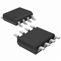
MAX410BESA Maxim Integrated Products, MAX410BESA Datasheet

MAX410BESA
Specifications of MAX410BESA
Related parts for MAX410BESA
MAX410BESA Summary of contents
Page 1
... Voltage Gain o Available in an Ultra-Small TDFN Package PART MAX410CPA MAX410BCPA MAX410CSA MAX410BCSA Applications MAX410EPA MAX410BEPA MAX410ESA MAX410BESA MAX410ETA MAX410MSA/PR MAX410MSA/PR Exposed pad. Top Mark—AGQ. ** Contact factory for availability. Ordering Information continued at end of data sheet. 42.2kΩ TOP VIEW 1% 6 ...
Page 2
Single/Dual/Quad, 28MHz, Low-Noise, Low-Voltage, Precision Op Amps ABSOLUTE MAXIMUM RATINGS Supply Voltage .......................................................................12V Differential Input Current (Note 1) ....................................±20mA Input Voltage Range........................................................ Common-Mode Input Voltage ..............(V+ + 0.3V) to (V- - 0.3V) Short-Circuit Current Duration....................................Continuous Continuous Power Dissipation ...
Page 3
Single/Dual/Quad, 28MHz, Low-Noise, ELECTRICAL CHARACTERISTICS (continued) ( -5V +25°C, unless otherwise noted.) A PARAMETER SYMBOL Operating Supply-Voltage Range Supply Current ELECTRICAL CHARACTERISTICS ( -5V 0°C to +70°C, unless ...
Page 4
Single/Dual/Quad, 28MHz, Low-Noise, Low-Voltage, Precision Op Amps ELECTRICAL CHARACTERISTICS (MAX410 only) ( -5V -55°C to +125°C, unless otherwise noted.) A PARAMETER SYMBOL Input Offset Voltage ∆V Offset Voltage Tempco Input Bias Current Input Offset ...
Page 5
Single/Dual/Quad, 28MHz, Low-Noise, ( -5V +25°C, unless otherwise noted.) = +25°C, unless otherwise noted VOLTAGE-NOISE DENSITY vs. FREQUENCY 100 = ± +25° 1/F CORNER = ...
Page 6
Single/Dual/Quad, 28MHz, Low-Noise, Low-Voltage, Precision Op Amps ( -5V +25°C, unless otherwise noted.) A SUPPLY CURRENT vs. TEMPERATURE 5 EACH AMPLIFIER = ± -60 - ...
Page 7
Single/Dual/Quad, 28MHz, Low-Noise, ( -5V +25°C, unless otherwise noted.) A TOTAL HARMONIC DISTORTION PLUS NOISE vs. FREQUENCY -85 = ±5V V 499Ω +25° P-P -91 -94 ...
Page 8
Single/Dual/Quad, 28MHz, Low-Noise, Low-Voltage, Precision Op Amps Applications Information The MAX410/MAX412/MAX414 provide low voltage- noise performance. Obtaining low voltage noise from a bipolar op amp requires high collector currents in the input stage, since voltage noise is inversely proportion- al ...
Page 9
Single/Dual/Quad, 28MHz, Low-Noise, 0.1µF 100kΩ 10Ω D.U.T Figure 3. 0.1Hz to 10Hz Voltage Noise Test Circuit 100 0.01 0.1 1 FREQUENCY (Hz) Figure 4. 0.1Hz to 10Hz Voltage Noise Test Circuit, Frequency Response circuit shown ...
Page 10
Single/Dual/Quad, 28MHz, Low-Noise, Low-Voltage, Precision Op Amps 909Ω +5V 0.022µ 10kΩ 100Ω D.U 0.022µF 10kΩ -5V Figure 5. Current-Noise Test Circuit Tech measures input-referred noise. For the circuit in Figure 5, assuming R is approximately equal ...
Page 11
Single/Dual/Quad, 28MHz, Low-Noise, 499Ω MAX410 MAX412 MAX414 R 10Ω D.U Figure 7a. Capacitive-Load Driving Circuit INPUT 1V/div OUTPUT 1V/div 1µs/div Figure 7b. Driving a 0.015µF Load with a 10Ω Isolation Resistor TDFN Exposed Paddle Connection On TDFN packages, ...
Page 12
Single/Dual/Quad, 28MHz, Low-Noise, Low-Voltage, Precision Op Amps Ordering Information (continued) PART TEMP RANGE MAX412CPA 0°C to +70°C MAX412BCPA 0°C to +70°C MAX412CSA 0°C to +70°C MAX412BCSA 0°C to +70°C MAX412EPA -40°C to +85°C MAX412BEPA -40°C to +85°C MAX412ESA -40°C to ...
Page 13
... Maxim cannot assume responsibility for use of any circuitry other than circuitry entirely embodied in a Maxim product. No circuit patent licenses are implied. Maxim reserves the right to change the circuitry and specifications without notice at any time. Maxim Integrated Products, 120 San Gabriel Drive, Sunnyvale, CA 94086 408-737-7600 ____________________ 13 © 2009 Maxim Integrated Products ...


