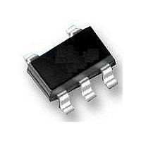
LMV931SN3T1G ON Semiconductor, LMV931SN3T1G Datasheet

LMV931SN3T1G
Specifications of LMV931SN3T1G
Available stocks
Related parts for LMV931SN3T1G
LMV931SN3T1G Summary of contents
Page 1
LMV931, LMV932 Single and Dual Low Voltage, Rail-to-Rail Input and Output, Operational Amplifiers The LMV931 Single and LMV932 Dual are CMOS low−voltage operational amplifiers which can operate on single−sided power supplies (1 5.0 V) with rail−to−rail input and ...
Page 2
SC70−5/TSOP− − 3 −IN (Top View) MAXIMUM RATINGS Symbol V Supply Voltage (Operating Range Input Differential Voltage IDR V Input Common Mode Voltage Range ICR Maximum Input Current t Output Short ...
Page 3
V DC ELECTRICAL CHARACTERISTICS + − 1 V+/ Parameter Symbol Input Offset Voltage V IO Input Offset Voltage TCV IO Average Drift Input Bias ...
Page 4
AC ELECTRICAL CHARACTERISTICS V− 2.0 V,Vo = V+/2 and R > 1 MW. Typical specifications represent the most likely parametric norm. Min/Max CM L specifications are guaranteed by testing, characterization, or statistical analysis. Parameter ...
Page 5
DC ELECTRICAL CHARACTERISTICS + − 2 V+/ Parameter Symbol Input Offset Voltage V IO Input Offset Voltage TCV IO Average Drift Input Bias Current ...
Page 6
AC ELECTRICAL CHARACTERISTICS V− 2.0V ,Vo = V+/2 and R > 1 MW. Typical specifications represent the most likely parametric norm. Min/Max CM L specifications are guaranteed by testing, characterization, or statistical analysis. Parameter ...
Page 7
DC ELECTRICAL CHARACTERISTICS − V+/ and R > 1 MW. Typical specifications represent the most likely parametric norm Parameter Symbol Input Offset Voltage V IO ...
Page 8
AC ELECTRICAL CHARACTERISTICS 2.0 V,Vo = V+/2 and R > 1 MW. Typical specifications represent the most likely parametric norm Parameter Symbol Slew Rate SR Gain Bandwidth GBWP Product Phase Margin Qm Gain ...
Page 9
A 0.12 LMV931 (Single) 25°C 0.1 0.08 125°C −40°C 0.06 0.04 0.02 0 1.8 2.2 2.6 3 3.4 3.8 SUPPLY VOLTAGE (V) Figure 2. Supply Current vs. Supply Voltage 100 1.8 ...
Page 10
TYPICAL CHARACTERISTICS (T = 25°C and unless otherwise specified Phase 40 30 Gain 200 1 610 ...
Page 11
TYPICAL CHARACTERISTICS (T = 25°C and unless otherwise specified Phase Gain 1 100 ...
Page 12
2 1 100 1000 FREQUENCY (Hz) Figure 11. CMRR vs. Frequency 10k 1k 100 100 1k ...
Page 13
TYPICAL CHARACTERISTICS (T = 25°C and unless otherwise specified 1 TIME (2ms/div) Figure 16. Small Signal Noninverting Response ...
Page 14
TYPICAL CHARACTERISTICS (T = 25°C and unless otherwise specified 5 TIME (2ms/div) Figure 18. Small Signal Noninverting Response ...
Page 15
TYPICAL CHARACTERISTICS (T = 25°C and unless otherwise specified 2 TIME (2ms/div) Figure 20. Large Signal Noninverting Response ...
Page 16
1 −40 − TEMPERATURE (°C) Figure 22. Short−Circuit vs. Temperature (Sinking 85°C 3 25°C ...
Page 17
... Figure 29. Comparator with Hysteresis ORDERING INFORMATION Number of Channels Order Number LMV931SQ3T2G Single LMV931SN3T1G Single LMV932DMR2G* Dual †For information on tape and reel specifications, including part orientation and tape sizes, please refer to our Tape and Reel Packaging Specifications Brochure, BRD8011/D. *Consult Sales. APPLICATION INFORMATION ...
Page 18
−B− 0.2 (0.008 PACKAGE DIMENSIONS SC−88A, SOT−353, SC−70 CASE 419A−02 ISSUE J NOTES: 1. DIMENSIONING AND TOLERANCING PER ANSI Y14.5M, 1982. 2. CONTROLLING DIMENSION: INCH. ...
Page 19
... A C SEATING 0.05 PLANE H T *For additional information on our Pb−Free strategy and soldering details, please download the ON Semiconductor Soldering and Mounting Techniques Reference Manual, SOLDERRM/D. PACKAGE DIMENSIONS TSOP−5 CASE 483−02 ISSUE H NOTES: 1. DIMENSIONING AND TOLERANCING PER 2. CONTROLLING DIMENSION: MILLIMETERS. ...
Page 20
... A 0.038 (0.0015) A1 *For additional information on our Pb−Free strategy and soldering details, please download the ON Semiconductor Soldering and Mounting Techniques Reference Manual, SOLDERRM/D. Micro8 is a trademark of International Rectifier. ON Semiconductor and are registered trademarks of Semiconductor Components Industries, LLC (SCILLC). SCILLC reserves the right to make changes without further notice to any products herein ...


