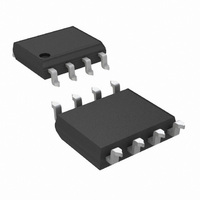
LMH6619MA/NOPB National Semiconductor, LMH6619MA/NOPB Datasheet - Page 24

LMH6619MA/NOPB
Manufacturer Part Number
LMH6619MA/NOPB
Description
IC AMP DUAL RRIO 130MHZ 8-SOIC
Manufacturer
National Semiconductor
Series
PowerWise®r
Specifications of LMH6619MA/NOPB
Amplifier Type
Voltage Feedback
Number Of Circuits
2
Output Type
Rail-to-Rail
Slew Rate
57 V/µs
Gain Bandwidth Product
58MHz
-3db Bandwidth
140MHz
Current - Input Bias
1.5µA
Voltage - Input Offset
100µV
Current - Supply
1.45mA
Current - Output / Channel
35mA
Voltage - Supply, Single/dual (±)
2.7 V ~ 11 V, ±1.35 V ~ 5.5 V
Operating Temperature
-40°C ~ 125°C
Mounting Type
Surface Mount
Package / Case
8-SOIC (3.9mm Width)
Bandwidth
130 MHz
Common Mode Rejection Ratio
96
Current, Input Bias
1 μA (NPN Active), -1.5 μA (PNP Active)
Current, Input Offset
0.01 μA
Current, Output
±35 mA
Current, Supply
1.3 mA
Impedance, Thermal
160 °C/W
Number Of Amplifiers
Dual
Package Type
SOIC-8
Resistance, Input
8 Megohms
Temperature, Operating, Range
-40 to +125 °C
Time, Fall
30 ns
Time, Rise
30 ns
Voltage, Gain
100 dB
Voltage, Input
2.7 to 11 V
Voltage, Noise
10 nV/sqrt Hz
Voltage, Offset
0.1 mV
Voltage, Output, High
230 mV
Voltage, Output, Low
255 mV
Voltage, Supply
5 V
Number Of Channels
2
Voltage Gain Db
100 dB
Common Mode Rejection Ratio (min)
81 dB
Input Offset Voltage
0.6 mV at 5 V
Operating Supply Voltage
3 V, 5 V, 9 V
Supply Current
3 mA at 5 V
Maximum Operating Temperature
+ 125 C
Minimum Operating Temperature
- 40 C
For Use With
551600075-001 - BOARD FOR SOIC LMH6612/19551600074-001 - BOARD FOR SOIC LMH6612/19
Lead Free Status / RoHS Status
Lead free / RoHS Compliant
Other names
LMH6619MA
www.national.com
CURRENT SENSE AMPLIFIER
With it’s rail-to-rail input and output capability, low V
low I
amplifier application. Figure 9 shows the schematic of the
LMH6618 set up in a low-side sense configuration which pro-
vides a conversion gain of 2V/A. Voltage error due to V
be
0.6 mV x 21 = 12.6 mV. Voltage error due to I
0.26 µA x 1 kΩ = 0.26 mV. Hence total voltage error is
12.6 mV + 0.26 mV or 12.86 mV which translates into a cur-
rent error of 12.86 mV/(2 V/A) = 6.43 mA.
TRANSIMPEDANCE AMPLIFIER
By definition, a photodiode produces either a current or volt-
age output from exposure to a light source. A Tran-
simpedance Amplifier (TIA) is utilized to convert this low-level
current to a usable voltage signal. The TIA often will need to
be compensated to insure proper operation.
Figure 10 shows the LMH6618 modeled with photodiode and
the internal op amp capacitances. The LMH6618 allows cir-
cuit operation of a low intensity light due to its low input bias
current by using larger values of gain (R
tance (C
the photodiode capacitance (C
of the op amp (C
portant role in the stability of the circuit. The noise gain of this
circuit determines the stability and is defined by:
FIGURE 10. Photodiode Modeled with Capacitance
B
calculated
the LMH6618 is an ideal choice for a current sense
T
) on the inverting terminal of the op amp includes
FIGURE 9. Current Sense Amplifier
IN
to
). This total capacitance (C
be
Elements
V
OS
PD
) and the input capacitance
x
(1
F
). The total capaci-
+
T
O
) plays an im-
20195862
is I
R
F
20195841
/R
O
OS
x R
G
OS
)
, and
F
can
or
or
24
FIGURE 11. Bode Plot of Noise Gain Intersecting with Op
Figure 11 shows the bode plot of the noise gain intersecting
the op amp open loop gain. With larger values of gain, C
R
the circuit can become unstable due to excess phase shift
around the loop.
A pole at f
feedback capacitor (C
flattened by choosing an appropriate value of C
performance.
Theoretical expressions for calculating the optimum value of
C
Equation 4 indicates that the −3 dB bandwidth of the TIA is
inversely proportional to the feedback resistor. Therefore, if
the bandwidth is important then the best approach would be
to have a moderate transimpedance gain stage followed by a
broadband voltage gain stage.
Table 3 shows the measurement results of the LMH6618 with
different photodiodes having various capacitances (C
a feedback resistance (R
F
F
create a zero in the transfer function. At higher frequencies
and the expected −3 dB bandwidth are:
P
in the noise gain function is created by placing a
Amp Open-Loop Gain
F
) across R
F
) of 1 kΩ.
F
. The noise gain slope is
F
for optimum
PD
20195865
T
) and
and
(1)
(2)
(3)
(4)


