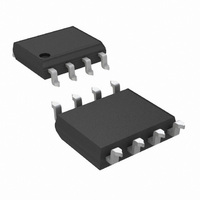
LMH6619MA/NOPB National Semiconductor, LMH6619MA/NOPB Datasheet - Page 23

LMH6619MA/NOPB
Manufacturer Part Number
LMH6619MA/NOPB
Description
IC AMP DUAL RRIO 130MHZ 8-SOIC
Manufacturer
National Semiconductor
Series
PowerWise®r
Specifications of LMH6619MA/NOPB
Amplifier Type
Voltage Feedback
Number Of Circuits
2
Output Type
Rail-to-Rail
Slew Rate
57 V/µs
Gain Bandwidth Product
58MHz
-3db Bandwidth
140MHz
Current - Input Bias
1.5µA
Voltage - Input Offset
100µV
Current - Supply
1.45mA
Current - Output / Channel
35mA
Voltage - Supply, Single/dual (±)
2.7 V ~ 11 V, ±1.35 V ~ 5.5 V
Operating Temperature
-40°C ~ 125°C
Mounting Type
Surface Mount
Package / Case
8-SOIC (3.9mm Width)
Bandwidth
130 MHz
Common Mode Rejection Ratio
96
Current, Input Bias
1 μA (NPN Active), -1.5 μA (PNP Active)
Current, Input Offset
0.01 μA
Current, Output
±35 mA
Current, Supply
1.3 mA
Impedance, Thermal
160 °C/W
Number Of Amplifiers
Dual
Package Type
SOIC-8
Resistance, Input
8 Megohms
Temperature, Operating, Range
-40 to +125 °C
Time, Fall
30 ns
Time, Rise
30 ns
Voltage, Gain
100 dB
Voltage, Input
2.7 to 11 V
Voltage, Noise
10 nV/sqrt Hz
Voltage, Offset
0.1 mV
Voltage, Output, High
230 mV
Voltage, Output, Low
255 mV
Voltage, Supply
5 V
Number Of Channels
2
Voltage Gain Db
100 dB
Common Mode Rejection Ratio (min)
81 dB
Input Offset Voltage
0.6 mV at 5 V
Operating Supply Voltage
3 V, 5 V, 9 V
Supply Current
3 mA at 5 V
Maximum Operating Temperature
+ 125 C
Minimum Operating Temperature
- 40 C
For Use With
551600075-001 - BOARD FOR SOIC LMH6612/19551600074-001 - BOARD FOR SOIC LMH6612/19
Lead Free Status / RoHS Status
Lead free / RoHS Compliant
Other names
LMH6619MA
DC LEVEL SHIFTING
Often a signal must be both amplified and level shifted while
using a single supply for the op amp. The circuit in Figure 7
can do both of these tasks. The procedure for specifying the
resistor values is as follows.
1.
2.
3.
4.
5.
6.
7.
8.
9.
10. Calculate R
11. Calculate R
12. Calculate R
Check that both the V
ranges of the LMH6618.
4
Figure 8 shows the LMH6619 used as the amplifier in a mul-
tiple feedback low pass filter. This filter is set up to have a gain
of +1 and a −3 dB point of 1 MHz. Values can be determined
th
ORDER MULTIPLE FEEDBACK LOW-PASS FILTER
Determine the input voltage.
Calculate the input voltage midpoint, V
(V
Determine the output voltage needed.
Calculate the output voltage midpoint, V
V
Calculate the gain needed, gain = (V
(V
Calculate the amount the voltage needs to be shifted
from input to output, ΔV
Set the supply voltage to be used.
Calculate the noise gain, noise gain = gain + ΔV
Set R
OUTMIN
INMAX
INMAX
F
.
– V
– V
+ (V
INMIN
INMIN
1
2
G
, R
, R
OUTMAX
, R
1
2
G
)/2.
)
= R
= R
= R
IN
– V
F
F
F
/gain.
/(noise gain-gain).
/(noise gain – 1).
and V
OUTMIN
OUT
= V
OUT
)/2.
FIGURE 8. 4
OUTMID
are within the voltage
OUTMAX
– gain x V
INMID
OUTMID
th
= V
– V
Order Multiple Feedback Low-Pass Filter
=
INMIN
OUTMIN
OUT
INMID
/V
+
.
S
)/
.
23
The following example is for a V
2V to 4V.
1.
2.
3.
4.
5.
6.
7.
8.
9.
10. R
11. R
12. R
by using the WEBENCH
amplifiers.national.com.
V
V
V
V
Gain = (4V – 2V)/(1V – 0V) = 2
ΔV
For the example the supply voltage will be +5V.
Noise gain = 2 + 2/5V = 2.4
R
IN
INMID
OUT
OUTMID
F
1
2
G
OUT
= 2 kΩ
= 2 kΩ/2 = 1 kΩ
= 2 kΩ/(2.4-2) = 5 kΩ
= 2 kΩ/(2.4 – 1) = 1.43 kΩ
= 0V to 1V
= 2V to 4V
= 0V + (1V – 0V)/2 = 0.5V
= 3V – 2 x 0.5V = 2
= 2V + (4V – 2V)/2 = 3V
FIGURE 7. DC Level Shifting
®
Active Filter Designer found at
IN
of 0V to 1V with a V
20195828
20195848
www.national.com
OUT
of


