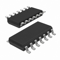
NE5234D/01,518 NXP Semiconductors, NE5234D/01,518 Datasheet - Page 5

NE5234D/01,518
Manufacturer Part Number
NE5234D/01,518
Description
IC OPAMP MATCHED QUAD HP 14SOIC
Manufacturer
NXP Semiconductors
Datasheet
1.NE5234D01518.pdf
(8 pages)
Specifications of NE5234D/01,518
Slew Rate
0.8 V/µs
Package / Case
14-SOIC (3.9mm Width), 14-SOL
Amplifier Type
General Purpose
Number Of Circuits
4
Output Type
Rail-to-Rail
-3db Bandwidth
2.5MHz
Current - Input Bias
90nA
Voltage - Input Offset
200µV
Current - Supply
2.8mA
Current - Output / Channel
12mA
Voltage - Supply, Single/dual (±)
2 V ~ 5.5 V, ±1 V ~ 2.75 V
Operating Temperature
0°C ~ 70°C
Mounting Type
Surface Mount
Number Of Channels
4
Common Mode Rejection Ratio (min)
65 dB
Input Offset Voltage
4 mV
Input Bias Current (max)
90 nA
Operating Supply Voltage
3 V, 5 V
Supply Current
4 mA
Maximum Power Dissipation
500 mW
Maximum Operating Temperature
+ 70 C
Minimum Operating Temperature
0 C
Maximum Dual Supply Voltage
+/- 2.75 V
Minimum Dual Supply Voltage
+/- 1 V
Mounting Style
SMD/SMT
Shutdown
No
Supply Voltage (max)
5.5 V
Supply Voltage (min)
2 V
Voltage Gain Db
110 dB
Lead Free Status / RoHS Status
Lead free / RoHS Compliant
Gain Bandwidth Product
-
Lead Free Status / Rohs Status
Lead free / RoHS Compliant
Other names
935275257518
NE5234D/01-T
NE5234D/01-T
NE5234D/01-T
NE5234D/01-T
1. These parameters are measured for V
Philips Semiconductors
DC ELECTRICAL CHARACTERISTICS (Continued)
NOTE:
AC ELECTRICAL CHARACTERISTICS
T
OUTPUT INVERSION PREVENTION
2002 Feb 22
SYMBOL
amb
SYMBOL
5 V
Matched quad high-performance
low-voltage operational amplifier
V
for common mode ranges between the measured regions.
A
THD
BW
SR
V
V
V
VOL
OUT
t
= +25 C; V
S
M
CC
GND
N
Open-loop voltage gain
Output voltage swing
Out ut voltage swing
Output voltage swing for
V
Slew rate
Unity gain bandwidth: –3 dB
Phase Margin
1% settling time
Input referred voltage noise
Total harmonic distortion
CC
CONVENTIONAL OP AMP
CC
= 2.75 V; V
V
IN
PARAMETER
= 2 V to 5.5 V; R
PARAMETER
g
V
OUT
EE
= –2.75 V
g
L
t
= 10 k ; C
EE
I
< V
Over full temperature
TEST CONDITIONS
TEST CONDITIONS
PEAK
temperature range
10 kHz, 1 V
Over full temperature
Over full temperature
TEST CONDITIONS
I
CM
I
A
PEAK
PEAK
L
V
R
A
Figure 2. Output inversion prevention.
R
= 5 mA over full
= 100 pF; unless otherwise stated.
< V
V
= 1; R
L
L
C
range
= 600
= 1, 1 V step
= 2 k
= 0.1 mA
L
= 10 mA
EE
range
range
1 kHz
= 50 pF
+0.5 V and for V
S
V
P-P
IN
= 0 , at
, A
47 k
47 k
V
= 1
V
V
V
V
V
5
EE
EE
EE
EE
EE
MIN
90
EE
+0.05
+0.25
+0.22
+0.25
+
–
MIN
+0.2
0.5
V
2
+1 V < V
CC
V
GND
NE5234
NE5234
TYP
110
90
TYP
0.8
2.5
1.4
0.1
55
25
CM
V
OUT
< V
V
V
V
V
V
CC
CC
CC
CC
CC
CC
MAX
MAX
4.0
. By design these parameters are intermediate
–0.05
–0.25
–0.25
–0.2
–0.2
LIMITS
LIMITS
V
V
MIN
V
V
V
0.5
EE
EE
2
EE
EE
EE
MIN
90
+0.25
+0.25
+0.1
+0.2
+0.2
V
IN
SA/SE5234
TYP
0.8
2.5
1.4
0.1
55
25
PHILIPS NE5234
SA5234
TYP
110
90
V
OUT
NE/SA5234
MAX
4.0
V
V
V
V
V
CC
CC
CC
CC
CC
MAX
t
–0.25
–0.25
–0.1
–0.2
–0.2
Product data
nV/Hz
UNITS
V/ s
MHz
deg
SL00569
%
V
V
s
CC
UNIT
GND
dB
1/2
V
V
V
V
5 V


