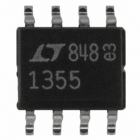
LT1355CS8 Linear Technology, LT1355CS8 Datasheet - Page 11

LT1355CS8
Manufacturer Part Number
LT1355CS8
Description
IC OP-AMP HISPD 12MHZ DUAL 8SOIC
Manufacturer
Linear Technology
Series
C-Load™r
Datasheet
1.LT1355CN8PBF.pdf
(16 pages)
Specifications of LT1355CS8
Amplifier Type
Voltage Feedback
Number Of Circuits
2
Slew Rate
400 V/µs
Gain Bandwidth Product
12MHz
Current - Input Bias
80nA
Voltage - Input Offset
300µV
Current - Supply
1mA
Current - Output / Channel
30mA
Voltage - Supply, Single/dual (±)
±2.5 V ~ 15 V
Operating Temperature
0°C ~ 70°C
Mounting Type
Surface Mount
Package / Case
8-SOIC (3.9mm Width)
Lead Free Status / RoHS Status
Contains lead / RoHS non-compliant
Output Type
-
-3db Bandwidth
-
Available stocks
Company
Part Number
Manufacturer
Quantity
Price
Part Number:
LT1355CS8
Manufacturer:
LT
Quantity:
20 000
Company:
Part Number:
LT1355CS8#PBF
Manufacturer:
LINEAR
Quantity:
29
Part Number:
LT1355CS8#TRPBF
Manufacturer:
LT
Quantity:
20 000
APPLICATIONS INFORMATION
SIMPLIFIED SCHEMATIC
The RC network across the output stage is bootstrapped
when the amplifi er is driving a light or moderate load and
has no effect under normal operation. When driving a ca-
pacitive load (or a low value resistive load) the network is
incompletely bootstrapped and adds to the compensation
at the high impedance node. The added capacitance slows
down the amplifi er which improves the phase margin by
moving the unity-gain frequency away from the pole formed
by the output impedance and the capacitive load. The zero
created by the RC combination adds phase to ensure that
even for very large load capacitances, the total phase lag
can never exceed 180 degrees (zero phase margin) and
the amplifi er remains stable.
Power Dissipation
The LT1355/LT1356 combine high speed and large output
drive in small packages. Because of the wide supply volt-
age range, it is possible to exceed the maximum junction
–IN
V
V
+
–
800Ω
R1
+IN
temperature under certain conditions. Maximum junction
temperature (T
ture (T
Worst-case power dissipation occurs at the maximum
supply current and when the output voltage is at 1/2 of
either supply voltage (or the maximum swing if less than
1/2 supply voltage). For each amplifi er P
Example: LT1356 in S16 at 70°C, V
LT1355CN8: T
LT1355CS8: T
LT1356CN:
LT1356CS:
P
P
T
JMAX
DMAX
DMAX
A
C
) and power dissipation (P
= 70°C + (4 • 99.8mW)(150°C/W) = 130°C
= (V
= (30V)(1.45mA) + (7.5V)
+
J
) is calculated from the ambient tempera-
– V
R
T
T
C
J
J
J
J
–
= T
= T
= T
= T
)(I
SMAX
A
A
A
A
+ (P
+ (P
+ (P
+ (P
LT1355/LT1356
) + (V
D
D
D
D
1355/1356 SS01
• 190°C/W)
• 150°C/W)
C
• 130°C/W)
• 110°C/W)
C
+
/2)
D
S
) as follows:
2
= ±15V, R
/1kW = 99.8mW
2
/R
L
DMAX
OUT
L
is:
= 1k
11
13556fb


