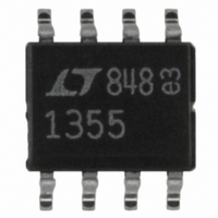
LT1355CS8 Linear Technology, LT1355CS8 Datasheet

LT1355CS8
Specifications of LT1355CS8
Available stocks
Related parts for LT1355CS8
LT1355CS8 Summary of contents
Page 1
... Singles, duals, and quads of each amplifi er are available. L, LT, LTC, LTM, Linear Technology and the Linear logo are registered trademarks of Linear Technology Corporation. C-Load is a trademark of Linear Technology Corporation. All other trademarks are the property of their respective owners. ...
Page 2
... JA ORDER INFORMATION LEAD FREE FINISH TAPE AND REEL LT1355CN8#PBF LT1355CN8#TRPBF LT1355CS8#PBF LT1355CS8#TRPBF LT1356CN#PBF LT1356CN#TRPBF LT1356CS#PBF LT1356CS#TRPBF Consult LTC Marketing for parts specifi ed with wider operating temperature ranges. Consult LTC Marketing for information on non-standard lead based fi nish parts. For more information on lead free part marking, go to: For more information on tape and reel specifi ...
Page 3
ELECTRICAL CHARACTERISTICS SYMBOL PARAMETER V Input Offset Voltage OS I Input Offset Current OS I Input Bias Current B e Input Noise Voltage n i Input Noise Current n R Input Resistance IN Input Resistance C Input Capacitance IN + ...
Page 4
LT1355/LT1356 ELECTRICAL CHARACTERISTICS SYMBOL PARAMETER Differential Gain Differential Phase R Output Resistance O Channel Separation I Supply Current S l The denotes the specifi cations which apply over the temperature range 0°C ≤ T SYMBOL PARAMETER V Input Offset Voltage ...
Page 5
ELECTRICAL CHARACTERISTICS –40°C ≤ T ≤ 85° unless otherwise noted. (Note SYMBOL PARAMETER V Input Offset Voltage OS Input V Drift OS I Input Offset Current OS I Input Bias Current B CMRR Common ...
Page 6
LT1355/LT1356 TYPICAL PERFORMANCE CHARACTERISTICS Supply Current vs Supply Voltage and Temperature 1.4 1.2 125°C 1.0 25°C 0.8 –55°C 0.6 0 SUPPLY VOLTAGE (±V) 1355/1356 G01 Input Bias Current vs Temperature 200 V = ±15V S + ...
Page 7
TYPICAL PERFORMANCE CHARACTERISTICS Output Short-Circuit Current vs Temperature ± SINK 40 SOURCE –50 – 100 TEMPERATURE (°C) 1355/1356 G10 Output Impedance vs Frequency 1k ...
Page 8
LT1355/LT1356 TYPICAL PERFORMANCE CHARACTERISTICS Gain and Phase vs Frequency 70 PHASE ±15V ±15V S 40 GAIN ± ± 25° ...
Page 9
TYPICAL PERFORMANCE CHARACTERISTICS 2nd and 3rd Harmonic Distortion vs Frequency – ±15V P-P – –40 3RD HARMONIC –50 –60 2ND HARMONIC –70 –80 100k 200k ...
Page 10
LT1355/LT1356 APPLICATIONS INFORMATION Layout and Passive Components The LT1355/LT1356 amplifi ers are easy to use and tolerant of less than ideal layouts. For maximum performance (for example, fast 0.01% settling) use a ground plane, short lead lengths, and RF-quality bypass ...
Page 11
... Maximum junction temperature (T ture (T ) and power dissipation (P A LT1355CN8: T LT1355CS8: T LT1356CN: LT1356CS: Worst-case power dissipation occurs at the maximum supply current and when the output voltage is at 1/2 of either supply voltage (or the maximum swing if less than 1/2 supply voltage). For each amplifi ...
Page 12
LT1355/LT1356 PACKAGE DESCRIPTION .300 – .325 (7.620 – 8.255) .008 – .015 (0.203 – 0.381) +.035 .325 –.015 +0.889 8.255 –0.381 NOTE: 1. DIMENSIONS ARE MILLIMETERS *THESE DIMENSIONS DO NOT INCLUDE MOLD FLASH OR PROTRUSIONS. MOLD FLASH OR PROTRUSIONS SHALL ...
Page 13
PACKAGE DESCRIPTION .300 – .325 (7.620 – 8.255) .008 – .015 (0.203 – 0.381) +.035 .325 –.015 +0.889 8.255 –0.381 NOTE: INCHES 1. DIMENSIONS ARE MILLIMETERS *THESE DIMENSIONS DO NOT INCLUDE MOLD FLASH OR PROTRUSIONS. MOLD FLASH OR PROTRUSIONS SHALL ...
Page 14
LT1355/LT1356 PACKAGE DESCRIPTION .050 BSC .245 MIN .030 .005 TYP RECOMMENDED SOLDER PAD LAYOUT .010 – .020 (0.254 – 0.508) .008 – .010 (0.203 – 0.254) (0.406 – 1.270) NOTE: 1. DIMENSIONS IN (MILLIMETERS) 2. DRAWING NOT TO SCALE 3. ...
Page 15
... MOLD FLASH OR PROTRUSIONS SHALL NOT EXCEED .006" (0.15mm) Information furnished by Linear Technology Corporation is believed to be accurate and reliable. However, no responsibility is assumed for its use. Linear Technology Corporation makes no representa- tion that the interconnection of its circuits as described herein will not infringe on existing patent rights. ...
Page 16
... COMMENTS Single Version of LT1355/LT1356 Lower Power Version of LT1355/LT1356, V Faster Version of LT1355/LT1356, V www.linear.com ● V OUT 1355/1356 TA03 – 1/2 V LT1355 OUT + C3 68pF 1355/1356 TA04 = 0.6mV 250µA/Amplifi 0.6mV 2mA/Amplifi 1009 REV B • PRINTED IN USA © LINEAR TECHNOLOGY CORPORATION 1994 13556fb ...


