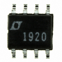
LT1920CS8 Linear Technology, LT1920CS8 Datasheet - Page 9

LT1920CS8
Manufacturer Part Number
LT1920CS8
Description
IC PREC INSTRUMNTATION AMP 8SOIC
Manufacturer
Linear Technology
Datasheet
1.LT1920CN8PBF.pdf
(12 pages)
Specifications of LT1920CS8
Amplifier Type
Instrumentation
Number Of Circuits
1
Slew Rate
1.2 V/µs
Gain Bandwidth Product
1MHz
Current - Input Bias
500pA
Voltage - Input Offset
30µV
Current - Supply
900µA
Current - Output / Channel
27mA
Voltage - Supply, Single/dual (±)
4.6 V ~ 36 V, ±2.3 V ~ 18 V
Operating Temperature
0°C ~ 70°C
Mounting Type
Surface Mount
Package / Case
8-SOIC (3.9mm Width)
Lead Free Status / RoHS Status
Contains lead / RoHS non-compliant
Output Type
-
-3db Bandwidth
-
Available stocks
Company
Part Number
Manufacturer
Quantity
Price
Part Number:
LT1920CS8
Manufacturer:
LINEAR/凌特
Quantity:
20 000
Company:
Part Number:
LT1920CS8#PBF
Manufacturer:
Avago
Quantity:
13 500
Part Number:
LT1920CS8#PBF
Manufacturer:
LINEAR/凌特
Quantity:
20 000
Part Number:
LT1920CS8#TRPBF
Manufacturer:
LINEAR/凌特
Quantity:
20 000
Input and Output Offset Voltage
The offset voltage of the LT1920 has two components: the
output offset and the input offset. The total offset voltage
referred to the input (RTI) is found by dividing the output
offset by the programmed gain (G) and adding it to the
input offset. At high gains the input offset voltage domi-
nates, whereas at low gains the output offset voltage
dominates. The total offset voltage is:
Reference Terminal
The reference terminal is one end of one of the four 10k
resistors around the difference amplifier. The output volt-
age of the LT1920 (Pin 6) is referenced to the voltage on
the reference terminal (Pin 5). Resistance in series with
the REF pin must be minimized for best common mode
rejection. For example, a 2 resistance from the REF pin
to ground will not only increase the gain error by 0.02%
but will lower the CMRR to 80dB.
Single Supply Operation
For single supply operation, the REF pin can be at the same
potential as the negative supply (Pin 4) provided the
output of the instrumentation amplifier remains inside the
specified operating range and that one of the inputs is at
least 2.5V above ground. The barometer application on the
front page of this data sheet is an example that satisfies
these conditions. The resistance R
transducer to ground sets the operating current for the
bridge and also has the effect of raising the input common
mode voltage. The output of the LT1920 is always inside
the specified range since the barometric pressure rarely
goes low enough to cause the output to rail (30.00 inches
of Hg corresponds to 3.000V). For applications that re-
quire the output to swing at or below the REF potential, the
voltage on the REF pin can be level shifted. An op amp is
used to buffer the voltage on the REF pin since a parasitic
series resistance will degrade the CMRR. The application
in the back of this data sheet, Four Digit Pressure Sensor,
is an example.
THEORY OF OPERATIO
Total input offset voltage (RTI)
= input offset + (output offset/G)
Total output offset voltage (RTO)
= (input offset • G) + output offset
SET
U
from the bridge
Output Offset Trimming
The LT1920 is laser trimmed for low offset voltage so that
no external offset trimming is required for most applica-
tions. In the event that the offset needs to be adjusted, the
circuit in Figure 2 is an example of an optional offset adjust
circuit. The op amp buffer provides a low impedance to the
REF pin where resistance must be kept to minimum for
best CMRR and lowest gain error.
Input Bias Current Return Path
The low input bias current of the LT1920 (2nA) and the
high input impedance (200G ) allow the use of high
impedance sources without introducing additional offset
voltage errors, even when the full common mode range is
required. However, a path must be provided for the input
bias currents of both inputs when a purely differential
signal is being amplified. Without this path the inputs will
float to either rail and exceed the input common mode
range of the LT1920, resulting in a saturated input stage.
Figure 3 shows three examples of an input bias current
path. The first example is of a purely differential signal
source with a 10k input current path to ground. Since the
impedance of the signal source is low, only one resistor is
needed. Two matching resistors are needed for higher
impedance signal sources as shown in the second
example. Balancing the input impedance improves both
common mode rejection and DC offset. The need for input
resistors is eliminated if a center tap is present as shown
in the third example.
–IN
+IN
Figure 2. Optional Trimming of Output Offset Voltage
R
G
2
1
8
3
–
+
LT1920
ADJUSTMENT RANGE
REF
5
10mV
1
6
LT1112
1/2
OUTPUT
–
+
2
3
10k
LT1920
V
V
+
–
10mV
100
100
–10mV
1920 F02
9


