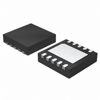
LT1995CDD#TRPBF Linear Technology, LT1995CDD#TRPBF Datasheet - Page 4

LT1995CDD#TRPBF
Manufacturer Part Number
LT1995CDD#TRPBF
Description
IC AMP GAIN SELECT 10-DFN
Manufacturer
Linear Technology
Datasheet
1.LT1995CMSPBF.pdf
(20 pages)
Specifications of LT1995CDD#TRPBF
Amplifier Type
Programmable Gain
Number Of Circuits
1
Slew Rate
1000 V/µs
-3db Bandwidth
32MHz
Voltage - Input Offset
750µV
Current - Supply
7.1mA
Current - Output / Channel
120mA
Voltage - Supply, Single/dual (±)
5 V ~ 30 V, ±2.5 V ~ 15 V
Operating Temperature
0°C ~ 70°C
Mounting Type
Surface Mount
Package / Case
10-WFDFN Exposed Pad
Lead Free Status / RoHS Status
Lead free / RoHS Compliant
Output Type
-
Gain Bandwidth Product
-
Current - Input Bias
-
Available stocks
Company
Part Number
Manufacturer
Quantity
Price
ELECTRICAL CHARACTERISTICS
LT1995
Difference Amplifier Configuration. V
SYMBOL
GE
V
V
V
CMRR
PSRR
V
I
SR
I
4
The
Difference Amplifier Configuration. V
SYMBOL
GE
SC
S
OS
OS
OS_OA
OUT
TC
●
denotes the specifications which apply over the –40°C ≤ T
PARAMETER
Gain Error
Input Offset Voltage
Referred to Input (Note 7)
Input Offset Voltage Drift
Referred to Input (Note 9)
Op Amp Input Offset Voltage
(Note 10)
Input Voltage Range
Common Mode Rejection Ratio
Referred to Input
Power Supply Rejection Ratio
Output Voltage Swing
Short-Circuit Current
Slew Rate
Supply Current
Gain Error
PARAMETER
REF
REF
CONDITIONS
V
V
V
V
V
G = 1 (MS10)
G = 1 (DD10)
G = 2 (MS10)
G = 2 (DD10)
G = 4 (MS10)
G = 4 (DD10)
G = 1 (MS10)
G = 1 (DD10)
G = 1 (MS10)
G = 1 (DD10)
G = 1 (MS10)
G = 1 (DD10)
G = 1 (MS10)
G = 1 (DD10)
G = 1
V
V
V
V
V
P1 = M1 = 0V, G = 1, V
R
R
R
R
G = 1
G = –2, V
Measured at V
G = 1
CONDITIONS
V
V
V
V
V
= V
= V
OUT
OUT
OUT
OUT
OUT
CM
CM
CM
CM
CM
L
L
L
L
OUT
OUT
OUT
OUT
OUT
= 1k
= 500Ω
= 500Ω
= 500Ω
CM
= ±15V, G = 1
= ±15V, G = 2
= ±15V, G = 4
= ±5V, G = 1
= ±1V, G = 1
CM
= ±12V, R
= ±12V, R
= ±12V, R
= ±2.5V, R
= ±2.5V, R
= ±12V, R
= ±12V, R
= ±12V, R
= ±2.5V, R
= ±2.5V R
= 0V and unused gain pins are unconnected, unless otherwise noted.
= 0V and unused gain pins are unconnected, unless otherwise noted.
OUT
= ±12V, P2 = 0V
OUT
L
L
L
L
L
L
L
L
L
L
= 1k, G = 1
= 1k, G = 2
= 1k, G = 4
= 1k, G = 1
= 1k, G = 2
= 1k, G = 4
= 150Ω, G = 1
= 500Ω, G = 1
= 150Ω, G = 1
= 500Ω, G = 1
= ±10V
The
S
= ±2.5V to ±15V
●
A
denotes the specifications which apply over the 0°C ≤ T
≤ 85°C.
V
±15V
±15V
±15V
±5V
±5V
±15V
±15V
±15V
±15V
±15V
±15V
±5V
±5V
±2.5V
±2.5V
±15V
±15V
±2.5V, ±5V, ±15V
±2.5V, ±5V, ±15V
±15V
±5V
±2.5V
±15V
±15V
±15V
±5V
±2.5V
±15V
±15V
±5V
±2.5V
±15V
±15V
±15V
±5V
V
±15V
±15V
±15V
±5V
±5V
SUPPLY
SUPPLY
●
●
●
●
●
●
●
●
●
●
●
●
●
●
●
●
●
●
●
●
●
●
●
●
●
●
●
●
●
●
●
●
●
●
●
●
●
●
●
●
●
±13.1
±12.6
MIN
±3.4
±1.2
±15
±55
600
MIN
±5
±1
63
69
73
62
59
76
±15.5
±13.5
±115
0.05
0.05
0.05
0.05
0.05
0.55
0.75
±5.5
±1.5
TYP
±14
900
0.05
0.05
0.05
0.05
0.05
TYP
1.1
1.5
0.8
1.2
0.7
0.9
1.4
1.3
7.9
7.4
10
10
77
83
86
72
66
86
±4
±2
1
1
MAX
0.25
0.25
0.25
0.25
0.35
11.5
11.5
11.5
3.25
5.75
10.5
MAX
A
0.35
0.35
6.5
5.5
7.5
6.5
6.5
9.9
26
35
0.3
0.3
0.5
9
5
≤ 70°C.
UNITS
UNITS
µV/°C
µV/°C
1995fb
V/µs
mV
mV
mV
mV
mV
mV
mV
mV
mV
mV
mV
mV
mA
mA
mA
dB
dB
dB
dB
dB
dB
%
%
%
%
%
%
%
%
%
%
V
V
V
V
V
V
V


