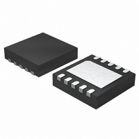
LT1995CDD#TRPBF Linear Technology, LT1995CDD#TRPBF Datasheet

LT1995CDD#TRPBF
Specifications of LT1995CDD#TRPBF
Available stocks
Related parts for LT1995CDD#TRPBF
LT1995CDD#TRPBF Summary of contents
Page 1
... MSOP and 10-Lead (3mm × 3mm) DFN packages. For a micropower precision amplifier with precision resistors, see the LT1991 and LT1996. , LTC and LT are registered trademarks of Linear Technology Corporation. All other trademarks are the property of their respective owners. OUT ...
Page 2
LT1995 ABSOLUTE MAXIMUM + – Total Supply Voltage ( .............................. 36V Input Current (Note 2) ....................................... ±10mA Output Short-Circuit Duration (Note 3) ........... Indefinite Operating Temperature Range (Note 4) .. – 40°C to 85°C ...
Page 3
ELECTRICAL CHARACTERISTICS Difference Amplifier Configuration 25° SYMBOL PARAMETER V Op Amp Input Offset Voltage OS_OA (Note 10) e Input Noise Voltage n R Common Mode Input Resistance Input Capacitance IN Input Voltage Range ...
Page 4
LT1995 ELECTRICAL CHARACTERISTICS Difference Amplifier Configuration. V REF SYMBOL PARAMETER GE Gain Error V Input Offset Voltage OS Referred to Input (Note Input Offset Voltage Drift OS Referred to Input (Note Amp Input Offset ...
Page 5
ELECTRICAL CHARACTERISTICS Difference Amplifier Configuration. V REF SYMBOL PARAMETER V Input Offset Voltage OS Referred to Input (Note Input Offset Voltage Drift OS Referred to Input (Note Amp Input Offset Voltage OS_OA (Note 10) ...
Page 6
LT1995 W U TYPICAL PERFOR A CE CHARACTERISTICS V Distribution ±15V PACKAGE –3.5 –1.5 –0.5 0.5 1.5 2.5 3.5 –2.5 INPUT OFFSET ...
Page 7
W U TYPICAL PERFOR A CE CHARACTERISTICS Gain vs Frequency –2 –4 = ±15V V S –6 ...
Page 8
LT1995 W U TYPICAL PERFOR A CE CHARACTERISTICS Power Supply Rejection Ratio vs Frequency 90 = ±15V 25° +PSRR 60 50 –PSRR –10 1k 10k ...
Page 9
W U TYPICAL PERFOR A CE CHARACTERISTICS Capacitive Load Handling 100 = ±15V 25° ∞ 10pF ...
Page 10
LT1995 CTIO S (Difference Amplifier Configuration) P1 (Pin 1): Noninverting Gain-of-1 Input. Connects a 4k internal resistor to the op amp’s noninverting input. P2 (Pin 2): Noninverting Gain-of-2 Input. Connects a 2k internal resistor to ...
Page 11
W BLOCK DIAGRA U U APPLICATIO S I FOR ATIO Configuration Flexibility The LT1995 combines a high speed precision operational amplifier with eight ratio-matched on-chip resistors. The resistor configuration and pinout of the device is shown in the Block Diagram. ...
Page 12
LT1995 U U APPLICATIO S I FOR ATIO As shown in Figure 1, the options for fixed gain G include: 1, 1.33, 1.67 and 7, all achieved by pin- strapping alone. With split-supply applications where ...
Page 13
U U APPLICATIO S I FOR ATIO + – LT1995 REF REF – 1. ...
Page 14
LT1995 U U APPLICATIO S I FOR ATIO + LT1995 1 P1 REF – 1. LT1995 ...
Page 15
U U APPLICATIO S I FOR ATIO + LT1995 REF – 0.875 + ...
Page 16
LT1995 U U APPLICATIO S I FOR ATIO Using the LT1995 as an AC-coupled inverting gain stage, the REF pin and the relevant P inputs may all be driven from a V source as depicted in the example of Figure ...
Page 17
U U APPLICATIO S I FOR ATIO If one of the A parameter configurations in Figure 3 is preferred, or the use of an external biasing source is desired, the P and REF input connections shown grounded in a Figure ...
Page 18
LT1995 U U APPLICATIO S I FOR ATIO and power dissipation ( follows for a nominal PCB D layout: • θ For example, in order to maintain a ...
Page 19
... RECOMMENDED SOLDER PAD PITCH AND DIMENSIONS Information furnished by Linear Technology Corporation is believed to be accurate and reliable. However, no responsibility is assumed for its use. Linear Technology Corporation makes no represen- tation that the interconnection of its circuits as described herein will not infringe on existing patent rights. ...
Page 20
... LT1995 + REF M1 SENSE – OUTPUT 100mV/A –15V 400mV V OUT f = 27MHz –3dB R = 75Ω L 10k 1995 TA06 Stable LOAD = 1.2mA, C Stable S LOAD LT/LT 0805 REV B • PRINTED IN THE USA © LINEAR TECHNOLOGY CORPORATION 2004 10k FLAG OUTPUT 4A LIMIT 1995 TA05 1995fb ...


