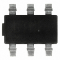
LT1395CS6#TRMPBF Linear Technology, LT1395CS6#TRMPBF Datasheet - Page 11

LT1395CS6#TRMPBF
Manufacturer Part Number
LT1395CS6#TRMPBF
Description
IC AMP CURR-FEEDBACK SGL SOT23-6
Manufacturer
Linear Technology
Datasheet
1.LT1396CDD.pdf
(20 pages)
Specifications of LT1395CS6#TRMPBF
Amplifier Type
Current Feedback
Number Of Circuits
1
Slew Rate
800 V/µs
-3db Bandwidth
400MHz
Current - Input Bias
10µA
Voltage - Input Offset
1000µV
Current - Supply
4.6mA
Current - Output / Channel
80mA
Voltage - Supply, Single/dual (±)
4 V ~ 12 V, ±2 V ~ 6 V
Operating Temperature
0°C ~ 70°C
Mounting Type
Surface Mount
Package / Case
SOT-23-6
Lead Free Status / RoHS Status
Lead free / RoHS Compliant
Output Type
-
Gain Bandwidth Product
-
Other names
LT1395CS6#TRMPBFTR
Available stocks
Company
Part Number
Manufacturer
Quantity
Price
APPLICATIONS INFORMATION
operation, it is important to keep the EN pin at least 3V
below the V
and the amplifi er will remain enabled at all times, then
the EN pin should be tied to the V
current is approximately 30μA when activated. If using
CMOS open-drain logic, an external 1k pull-up resistor
is recommended to ensure that the LT1395CS6 remains
disabled in spite of any CMOS drain leakage currents.
The enable/disable times are very fast when driven from
standard 5V CMOS logic. The LT1395CS6 enables in about
30ns (50% point to 50% point) while operating on ±5V
supplies (Figure 2). Likewise, the disable time is approxi-
mately 40ns (50% point to 50% point) (Figure 3).
V
V
V
V
Figure 3. Amplifi er Disable Time, A
S
IN
Figure 2. Amplifi er Enable Time, A
S
IN
= ±5V
= ±5V
+
= 1V
= 1V
supply. If a V
R
R
R
R
F
G
F
G
= 255Ω
= 255Ω
= 255Ω
= 255Ω
R
R
+
L
L
= 100Ω
= 100Ω
of less than 3V is desired,
–
supply. The enable pin
1395/6/7 F02
1395/6/7 F03
V
V
= 2
= 2
OUTPUT
EN
OUTPUT
EN
SOURCES
R
G
B
Differential Input Signal Swing
To avoid any breakdown condition on the input transis-
tors, the differential input swing must be limited to ± 5V.
In normal operation, the differential voltage between the
input pins is small, so the ±5V limit is not an issue.
Buffered RGB to Color-Difference Matrix
An LT1397 can be used to create buffered color-difference
signals from RGB inputs (Figure 4). In this application,
the R input arrives via 75Ω coax. It is routed to the non-
inverting input of LT1397 amplifi er A1 and to a 845Ω
resistor R8. There is also an 82.5Ω termination resistor
R11, which yields a 75Ω input impedance at the R input
when considered in parallel with R8. R8 connects to
the inverting input of a second LT1397 amplifi er (A2),
which also sums the weighted G and B inputs to create a
–0.5 • Y output. LT1397 amplifi er A3 then takes the
–0.5 • Y output and amplifi es it by a gain of –2, resulting
in the Y output. Amplifi er A1 is confi gured in a noninvert-
ing gain of 2 with the bottom of the gain resistor R2 tied
to the Y output. The output of amplifi er A1 thus results
in the color-difference output R-Y.
The B input is similar to the R input. It arrives via 75Ω
coax, and is routed to the noninverting input of LT1397
amplifi er A4, and to a 2320Ω resistor R10. There is also
a 76.8Ω termination resistor R13, which yields a 75Ω
75Ω
Figure 4. Buffered RGB to Color-Difference Matrix
ALL RESISTORS 1%
V
S
R11
82.5Ω
R12
90.9Ω
R13
76.8Ω
= ±5V
LT1395/LT1396/LT1397
2320Ω
845Ω
432Ω
R10
R8
R9
1/4 LT1397
–
+
A2
255Ω
R7
127Ω
R6
1/4 LT1397
1/4 LT1397
+
1/4 LT1397
–
–
+
–
+
A4
A3
A1
255Ω
R5
11
1395/6/7 F04
R1
255Ω
R2
255Ω
R4
255Ω
R3
255Ω
139567fd
R-Y
Y
B-Y


