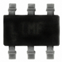
LT1395CS6#TRM Linear Technology, LT1395CS6#TRM Datasheet

LT1395CS6#TRM
Specifications of LT1395CS6#TRM
Available stocks
Related parts for LT1395CS6#TRM
LT1395CS6#TRM Summary of contents
Page 1
... Technology’s proprietary complementary bipolar process. They have standard single/dual/quad pinouts and they are optimized for use on supply voltages of ±5V. L, LT, LTC, LTM, Linear Technology and the Linear logo are registered trademarks of Linear Technology Corporation. All other trademarks are the property of their respective owners. R ...
Page 2
LT1395/LT1396/LT1397 ABSOLUTE MAXIMUM RATINGS + – Total Supply Voltage ( .............................12.6V Input Current (Note 2) ......................................... ±10mA Output Current .................................................. ±100mA Differential Input Voltage (Note 2).............................±5V Output Short-Circuit Duration (Note 3) ........ Continuous Operating Temperature Range (Note ...
Page 3
PIN CONFIGURATION TOP VIEW + OUT – – + –IN S6 PACKAGE 6-LEAD PLASTIC TSOT-23 = 150°C, θ 230°C/W JMAX JA ORDER INFORMATION LEAD FREE FINISH TAPE AND ...
Page 4
LT1395/LT1396/LT1397 ELECTRICAL CHARACTERISTICS The denotes specifi cations which apply over the specifi ed operating temperature range, otherwise specifi cations are at T ● = ±5V 0.5V, pulse tested, unless otherwise noted. (Note 5) For each amplifi er: V ...
Page 5
ELECTRICAL CHARACTERISTICS The denotes specifi cations which apply over the specifi ed operating temperature range, otherwise specifi cations are at T ● For each amplifi ±5V, pulse tested, unless otherwise noted. (Note 5) CM ...
Page 6
LT1395/LT1396/LT1397 TYPICAL AC PERFORMANCE V ( (Ω ±5 1 100 ±5 2 100 ±5 –1 100 ±5 3 500 ±5 5 500 ±5 10 500 ±5 10 500 TYPICAL PERFORMANCE CHARACTERISTICS Closed-Loop Gain vs Frequency ...
Page 7
TYPICAL PERFORMANCE CHARACTERISTICS 2nd and 3rd Harmonic Distortion vs Frequency 25° 255W 100Ω ± 2VPP OUT 60 70 HD3 HD2 ...
Page 8
LT1395/LT1396/LT1397 TYPICAL PERFORMANCE CHARACTERISTICS Output Voltage Swing vs Temperature 100k R = 150Ω ±5V S –1 –2 – 100k R = 150Ω –4 –5 ...
Page 9
PIN FUNCTIONS LT1395CS5 OUT (Pin 1): Output. – V (Pin 2): Negative Supply Voltage, Usually –5V. +IN (Pin 3): Noninverting Input. – IN (Pin 4): Inverting Input (Pin 5): Positive Supply Voltage, Usually 5V. LT1395CS6 OUT (Pin 1): ...
Page 10
LT1395/LT1396/LT1397 APPLICATIONS INFORMATION Feedback Resistor Selection The small-signal bandwidth of the LT1395/LT1396/LT1397 is set by the external feedback resistors and the inter- nal junction capacitors result, the bandwidth is a function of the supply voltage, the value of ...
Page 11
APPLICATIONS INFORMATION V = ± 255Ω 100Ω 255Ω Figure 2. Amplifi er Enable Time ± 255Ω 100Ω ...
Page 12
LT1395/LT1396/LT1397 APPLICATIONS INFORMATION input impedance when considered in parallel with R10. R10 also connects to the inverting input of amplifi er A2, adding the B contribution to the Y signal as discussed above. Amplifi confi gured in ...
Page 13
SIMPLIFIED SCHEMATIC EN (LT1395CS6 ONLY) FOR ALL NON-DISABLE DEVICES PACKAGE DESCRIPTION 3.5 0.05 1.65 0.05 2.10 0.05 (2 SIDES) 0.25 0.05 0.50 BSC 2.38 0.05 RECOMMENDED SOLDER PAD PITCH AND DIMENSIONS APPLY SOLDER MASK TO AREAS THAT ARE NOT SOLDERED ...
Page 14
LT1395/LT1396/LT1397 PACKAGE DESCRIPTION 3.30 0.05 3.60 0.05 2.20 0.05 1.70 0.05 0.25 0.05 0.50 BSC 3.00 REF RECOMMENDED SOLDER PAD PITCH AND DIMENSIONS APPLY SOLDER MASK TO AREAS THAT ARE NOT SOLDERED NOTE: 1. DRAWING PROPOSED TO BE MADE VARIATION ...
Page 15
PACKAGE DESCRIPTION 5.23 (.206) MIN 0.42 0.038 (.0165 .0015) TYP RECOMMENDED SOLDER PAD LAYOUT 0.254 (.010) GAUGE PLANE 0.18 (.007) NOTE: 1. DIMENSIONS IN MILLIMETER/(INCH) 2. DRAWING NOT TO SCALE 3. DIMENSION DOES NOT INCLUDE MOLD FLASH, PROTRUSIONS OR GATE ...
Page 16
LT1395/LT1396/LT1397 PACKAGE DESCRIPTION 0.62 MAX 3.85 MAX 2.62 REF RECOMMENDED SOLDER PAD LAYOUT PER IPC CALCULATOR 0.20 BSC DATUM ‘A’ 0.30 – 0.50 REF NOTE: 1. DIMENSIONS ARE IN MILLIMETERS 2. DRAWING NOT TO SCALE 3. DIMENSIONS ARE INCLUSIVE OF ...
Page 17
PACKAGE DESCRIPTION 0.62 0.95 MAX REF 3.85 MAX 2.62 REF RECOMMENDED SOLDER PAD LAYOUT PER IPC CALCULATOR 0.20 BSC DATUM ‘A’ 0.30 – 0.50 REF NOTE: 1. DIMENSIONS ARE IN MILLIMETERS 2. DRAWING NOT TO SCALE 3. DIMENSIONS ARE INCLUSIVE ...
Page 18
LT1395/LT1396/LT1397 PACKAGE DESCRIPTION .050 BSC .245 MIN .030 ±.005 TYP RECOMMENDED SOLDER PAD LAYOUT .010 – .020 (0.254 – 0.508) .008 – .010 (0.203 – 0.254) (0.406 – 1.270) NOTE: 1. DIMENSIONS IN (MILLIMETERS) 2. DRAWING NOT TO SCALE 3. ...
Page 19
PACKAGE DESCRIPTION .050 BSC N .245 MIN .030 ±.005 TYP RECOMMENDED SOLDER PAD LAYOUT .010 – .020 45° (0.254 – 0.508) .008 – .010 (0.203 – 0.254) .016 – .050 (0.406 – 1.270) NOTE: INCHES 1. DIMENSIONS ...
Page 20
... Switching Time, 250MHz Bandwidth 300MHz Bandwidth, Specifi +5V and ±5V, 3mm × 3mm QFN Package www.linear.com ● , with a source impedance IN with no additional IN equals a buffered ver- OUT OUT 1N4148 75Ω 1395/6/7 TA03 LT 0709 REV D • PRINTED IN USA © LINEAR TECHNOLOGY CORPORATION 1999 139567fd ...


