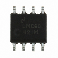
LMC6042IM/NOPB National Semiconductor, LMC6042IM/NOPB Datasheet - Page 4

LMC6042IM/NOPB
Manufacturer Part Number
LMC6042IM/NOPB
Description
IC OP AMP CMOS DUAL MICRO 8-SOIC
Manufacturer
National Semiconductor
Datasheet
1.LMC6042INNOPB.pdf
(15 pages)
Specifications of LMC6042IM/NOPB
Amplifier Type
General Purpose
Number Of Circuits
2
Output Type
Rail-to-Rail
Slew Rate
0.02 V/µs
Gain Bandwidth Product
100kHz
Current - Input Bias
0.002pA
Voltage - Input Offset
1000µV
Current - Supply
26µA
Current - Output / Channel
40mA
Voltage - Supply, Single/dual (±)
4.5 V ~ 15.5 V, ±2.25 V ~ 7.75 V
Operating Temperature
-40°C ~ 85°C
Mounting Type
Surface Mount
Package / Case
8-SOIC (3.9mm Width)
Lead Free Status / RoHS Status
Lead free / RoHS Compliant
-3db Bandwidth
-
Other names
*LMC6042IM
*LMC6042IM/NOPB
LMC6042IM
*LMC6042IM/NOPB
LMC6042IM
www.national.com
T.H.D.
Symbol
AC Electrical Characteristics
Unless otherwise specified, all limits guaranteed for T
5V, V
Note 1: Absolute Maximum Ratings indicate limits beyond which damage to the device may occur. Operating Conditions indicate conditions for which the device
is intended to be functional, but do not guarantee specific performance limits. For guaranteed specifications and test conditions, see the Electrical Characteristics.
The guaranteed specifications apply only for the test conditions listed.
Note 2: Applies to both single-supply operation. Continuous short circuit operation at elevated ambient temperature can result in exceeding the maximum allowed
junction temperature of 110˚C. Output currents in excess of
Note 3: The maximum power dissipation is a function of T
− T
Note 4: Human body model, 1.5 kΩ in series with 100 pF.
Note 5: Typical values represent the most likely parametric norm.
Note 6: All limits are guaranteed at room temperature (standard type face) or at operating temperature extremes (bold face type).
Note 7: V
Note 8: V
Note 9: Input referred V
Note 10: For operating at elevated temperatures the device must be derated based on the thermal resistance θ
Note 11: All numbers apply for packages soldered directly into a PC board.
Note 12: Do not connect output to V
Typical Performance Characteristics
V
A
S
)/θ
=
−
JA
±
.
= 0V, V
+
+
7.5V, T
= 15V, V
= 15V. Connected as Voltage Follower with 10V step input. Number specified is the slower of the positive and negative slew rates.
Total Harmonic Distortion
CM
A
CM
= 25˚C unless otherwise specified
= 1.5V, V
= 7.5V and R
+
Parameter
= 15V and R
Supply Current vs
Supply Voltage
O
+
L
when V
= V
L
connected to 7.5V. For Sourcing tests, 7.5V ≤ V
= 100 kΩ connected to V
+
/2 and R
+
is greater than 13V or reliability may be adversely affected.
f = 1 kHz, A
R
±
L
01113719
L
5V Supply
J(Max)
>
= 100 kΩ, V
±
1M unless otherwise specified.
30 mA over long term may adversely affect reliability.
, θ
(Continued)
JA
Conditions
+
, and T
/2. Each amp excited in turn with 100 Hz to produce V
A
V
= T
= −5
A
O
J
. The maximum allowable power dissipation at any ambient temperature is P
= 25˚C. Boldface limits apply at the temperature extremes. V
= 2 V
4
PP
O
≤ 11.5V. For Sinking tests, 2.5V ≤ V
(Note 5)
0.01
Typ
Representative Units
Temperature of Five
Offset Voltage vs
JA
LMC6042AI
(Note 6)
with P
Limit
D
O
= (T
= 12 V
O
J
≤ 7.5V.
− T
PP
LMC6042I
A
.
)/θ
(Note 6)
Limit
JA
.
01113720
D
= (T
(Limit)
Units
%
J(Max)
+
=


