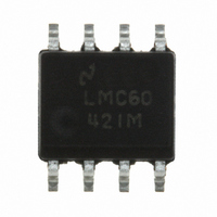
LMC6042IM/NOPB National Semiconductor, LMC6042IM/NOPB Datasheet - Page 11

LMC6042IM/NOPB
Manufacturer Part Number
LMC6042IM/NOPB
Description
IC OP AMP CMOS DUAL MICRO 8-SOIC
Manufacturer
National Semiconductor
Datasheet
1.LMC6042INNOPB.pdf
(15 pages)
Specifications of LMC6042IM/NOPB
Amplifier Type
General Purpose
Number Of Circuits
2
Output Type
Rail-to-Rail
Slew Rate
0.02 V/µs
Gain Bandwidth Product
100kHz
Current - Input Bias
0.002pA
Voltage - Input Offset
1000µV
Current - Supply
26µA
Current - Output / Channel
40mA
Voltage - Supply, Single/dual (±)
4.5 V ~ 15.5 V, ±2.25 V ~ 7.75 V
Operating Temperature
-40°C ~ 85°C
Mounting Type
Surface Mount
Package / Case
8-SOIC (3.9mm Width)
Lead Free Status / RoHS Status
Lead free / RoHS Compliant
-3db Bandwidth
-
Other names
*LMC6042IM
*LMC6042IM/NOPB
LMC6042IM
*LMC6042IM/NOPB
LMC6042IM
Applications Hints
The designer should be aware that when it is inappropriate
to lay out a PC board for the sake of just a few circuits, there
is another technique which is even better than a guard ring
on a PC board: Don’t insert the amplifier’s input pin into the
board at all, but bend it up in the air and use only air as an
insulator. Air is an excellent insulator. In this case you may
have to forego some of the advantages of PC board con-
struction, but the advantages are sometimes well worth the
effort of using point-to-point up-in-the-air wiring. See Figure
6.
(Input pins are lifted out of PC board and soldered directly to components.
All other pins connected to PC board.)
Typical Single-Supply Applications
The extremely high input impedance, and low power con-
sumption, of the LMC6042 make it ideal for applications that
require battery-powered instrumentation amplifiers. Ex-
amples of these types of applications are hand-held pH
probes, analytic medical instruments, magnetic field detec-
tors, gas detectors, and silicon based pressure transducers.
The circuit in Figure 7 is recommended for applications
where the common-mode input range is relatively low and
(V
+
= 5.0 V
DC
)
FIGURE 6. Air Wiring
(Continued)
FIGURE 7. Two Op-Amp Instrumentation Amplifier
01113711
11
the differential gain will be in the range of 10 to 1000. This
two op-amp instrumentation amplifier features an indepen-
dent adjustment of the gain and common-mode rejection
trim, and a total quiescent supply current of less than 20 µA.
To maintain ultra-high input impedance, it is advisable to use
ground rings and consider PC board layout an important part
of the overall system design (see Printed-Circuit-Board Lay-
out for High Impedance Work). Referring to Figure 7, the
input voltages are represented as a common-mode input
V
Rejection of the common-mode component of the input is
accomplished by making the ratio of R1/R2 equal to R3/R4.
So that where,
A suggested design guideline is to minimize the difference of
value between R1 through R4. This will often result in im-
proved resistor tempco, amplifier gain, and CMRR over tem-
perature. If RN = R1 = R2 = R3 = R4 then the gain equation
can be simplified:
Due to the “zero-in, zero-out” performance of the LMC6042,
and output swing rail-rail, the dynamic range is only limited to
the input common-mode range of 0V to V
case at room temperature. This feature of the LMC6042
makes it an ideal choice for low-power instrumentation sys-
tems.
A complete instrumentation amplifier designed for a gain of
100 is shown in Figure 8. Provisions have been made for low
sensitivity trimming of CMRR and gain.
CM
plus a differential input V
01113712
D
.
S
− 2.3V, worst
www.national.com


