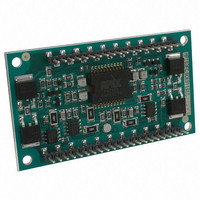
MP103FC Cirrus Logic Inc, MP103FC Datasheet - Page 5

MP103FC
Manufacturer Part Number
MP103FC
Description
HIGH POWER AMP MODULE 65V/USSLEW
Manufacturer
Cirrus Logic Inc
Series
Apex Precision Power™r
Specifications of MP103FC
Amplifier Type
Power
Number Of Circuits
2
Slew Rate
167 V/µs
-3db Bandwidth
230kHz
Current - Input Bias
3.3µA
Voltage - Input Offset
2000µV
Current - Supply
19mA
Current - Output / Channel
12A
Voltage - Supply, Single/dual (±)
30 V ~ 200 V, ±15 V ~ 100 V
Operating Temperature
0°C ~ 70°C
Mounting Type
Through Hole
Package / Case
42-DIP Module
Input Voltage Range (max)
200 V
Input Voltage Range (min)
20 V
Input Offset Voltage
2 mV
Output Current (typ)
15 A
Supply Current
1 mA
Maximum Power Dissipation
35 W
Maximum Operating Temperature
+ 70 C
Minimum Operating Temperature
0 C
Lead Free Status / RoHS Status
Contains lead / RoHS non-compliant
Output Type
-
Gain Bandwidth Product
-
Lead Free Status / Rohs Status
No
Other names
598-1794
MP103FC
Q4110212
MP103FC
Q4110212
Available stocks
Company
Part Number
Manufacturer
Quantity
Price
Company:
Part Number:
MP103FC
Manufacturer:
Cirrus
Quantity:
145
Part Number:
MP103FC
Manufacturer:
APEX
Quantity:
20 000
GENERAL
Please read Application Note 1 “General Operating Considerations” which covers stability, power supplies, heat
sinking, mounting, current limit, SOA interpretation, and specification interpretation. Visit www.Cirrus.com for design
tools that help automate tasks such as calculations for stability, internal power dissipation, current limit, heat sink
selection, Apex Precision Power’s complete Application Notes library, Technical Seminar Workbook and Evaluation
Kits.
AMPLIFIER GAIN
When the feedback pin for each channel is connected to the corresponding OUT pin, the gain of the amplifier is
internally set to 65 V/V. The amplifier gain can be increased by connecting a resistor between the feedback and Out
pin. The amplifier gain will be increased approximately 1 V/V for each additional 49.9Ω added between the feedback
and OUT pin.
SAFE OPERATING AREA
The MOSFET output stage of the MP103 is not limited by second breakdown considerations as in bipolar output
stages. Only thermal considerations and current handling capabilities limit the SOA (see Safe Operating Area
graph). The output stage is protected against transient flyback by the parasitic body diodes of the output stage
MOSFET structure. However, for protection against sustained high energy flyback external fast-recovery diodes
must be used.
POWER SUPPLY BYPASSING
Bypass capacitors to power supply terminals +V
local parasitic oscillation in the output stage of the MP103. Use electrolytic capacitors at least 10μF per output amp
required. Bypass the electrolytic capacitors with high quality ceramic capacitors (X7R) 0.1μF or greater. Duplicate
the supply bypass for the supply terminals of each amplifier channel. A bypass capacitor of 0.1μF or greater is rec-
ommended for the +V
CURRENT LIMIT
For proper operation, the current limit resistor (R
gram. For optimum reliability the resistor value should be set as high as possible. The value is calculated as follows;
with the maximum practical value of 30Ω. The current limit function can be disabled by shorting the I
pin.
POWER SUPPLY PROTECTION
Unidirectional zener diode transient suppressors are recommended as protection on the supply pins. The zeners
clamp transients to voltages within the power supply rating and also clamp power supply reversals to ground.
Whether the zeners are used or not, the system power supply should be evaluated for transient performance in-
cluding power-on overshoot and power-off polarity reversal as well as line regulation. Conditions which can cause
open circuits or polarity reversals on either power supply rail should be avoided or protected against. Reversals or
opens on the negative supply rail is known to induce input stage failure. Unidirectional transzorbs prevent this, and
it is desirable that they be both electrically and physically as close to the amplifier as possible.
SERIES ISOLATION RESISTOR, R
To insure stability with all capacitive loads a series isolation resistor should be included between the output and the
load as shown in the external connections drawing. A 1Ω resistor works well for capacitive loads between 135pF
and 44nF. The resistor will affect the rise and fall time of the output pulse at the capacitive load. This can be com-
pensated for on the input signal.
BACKPLATE GROUNDING
The substrate of the MP103 is an insulated metal substrate. It is required that it be connected to signal ground. This
is accomplished when the ground pin (Pin 32) is properly connected signal ground.
MP103U
P r o d u c t T e c h n o l o g y F r o m
AUX
terminal.
S
S
and -V
LIM
R
) must be connected as shown in the external connection dia-
LIM
= 0.7/I
S
must be connected physically close to the pins to prevent
LIM
L
pin to the OUT
MP103
5


