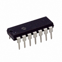
MCP619-I/P Microchip Technology, MCP619-I/P Datasheet - Page 13

MCP619-I/P
Manufacturer Part Number
MCP619-I/P
Description
IC OPAMP 2.3V QUAD R-R 14DIP
Manufacturer
Microchip Technology
Specifications of MCP619-I/P
Slew Rate
0.08 V/µs
Operating Temperature
-40°C ~ 85°C
Amplifier Type
General Purpose
Number Of Circuits
4
Output Type
Rail-to-Rail
Gain Bandwidth Product
190kHz
Current - Input Bias
15nA
Voltage - Input Offset
150µV
Current - Supply
19µA
Current - Output / Channel
17mA
Voltage - Supply, Single/dual (±)
2.3 V ~ 5.5 V
Mounting Type
Through Hole
Package / Case
14-DIP (0.300", 7.62mm)
Op Amp Type
General Purpose
No. Of Amplifiers
4
Bandwidth
190kHz
Supply Voltage Range
2.3V To 5.5V
Amplifier Case Style
DIP
No. Of Pins
14
Number Of Channels
4
Voltage Gain Db
120 dB
Common Mode Rejection Ratio (min)
80 dB
Input Offset Voltage
0.15 mV
Operating Supply Voltage
3 V, 5 V
Maximum Operating Temperature
+ 85 C
Mounting Style
Through Hole
Minimum Operating Temperature
- 40 C
Lead Free Status / RoHS Status
Lead free / RoHS Compliant
-3db Bandwidth
-
Lead Free Status / Rohs Status
Details
Available stocks
Company
Part Number
Manufacturer
Quantity
Price
Company:
Part Number:
MCP619-I/P
Manufacturer:
MICROCHIP
Quantity:
12 000
Part Number:
MCP619-I/P
Manufacturer:
MICROCHIP/微芯
Quantity:
20 000
Now calculate the nominal DC bias point with offset:
EQUATION 4-1:
Use the worst-case specs and source values to
determine the worst-case
offset
input voltage range and output voltage range are not
exceeded.
4.3
There are two specifications that describe the output
swing capability of the MCP616/7/8/9 family of op
amps. The first specification (Maximum Output Voltage
Swing) defines the absolute maximum swing that can
be achieved under the specified load conditions. For
instance, the output voltage swings to within 15 mV of
the negative rail with a 25 k
Figure 2-33 shows how the output voltage is limited
when the input goes beyond the linear region of
operation.
The second specification that describes the output
swing capability of these amplifiers is the Linear Output
Voltage
maximum output swing that can be achieved while the
amplifier still operates in its linear region. To verify
linear operation in this range, the large-signal DC
Open-Loop Gain (A
supply rails. The measurement must meet the specified
A
4.4
Driving large capacitive loads can cause stability
problems for voltage feedback op amps. As the load
capacitance increases, the feedback loop’s phase
margin decreases and the closed-loop bandwidth is
reduced. This produces gain peaking in the frequency
response, with overshoot and ringing in the step
© 2005 Microchip Technology Inc.
Where:
OL
conditions in the specification table.
G
V
V
I
I
V
G
V
V
V
B
OS
for your design. Make sure the common mode
OOS
OS
CM
OOS
CM
OUT
N
N
Rail-to-Rail Output
Capacitive Loads
=
Range.
= V
= G
= V
1
= op amp’s noise gain (from the
= circuit’s output offset voltage
= op amp’s input offset voltage
= op amp’s input bias current
= op amp’s input offset current
= op amp’s common mode input
+
EQ
EQ
N
non-inverting input to the output)
voltage
R
[V
– (I
2
(G
OS
OL
This
R
B
N
1
+ I
) is measured at points inside the
+ I
) – V
– I
B
OS
OS
output voltage range and
((R
1
specification
((R
/2) R
(G
1
N
1
||R
||R
EQ
– 1) + V
2
load tied to V
2
) – R
) + R
EQ
OOS
EQ
defines
)
) / 2]
DD
the
/2.
response. A unity-gain buffer (G = +1) is the most
sensitive to capacitive loads, though all gains show the
same general behavior.
When driving large capacitive loads with these op
amps (e.g., > 60 pF when G = +1), a small series
resistor at the output (R
feedback loop’s phase margin (stability) by making the
output load resistive at higher frequencies. The
bandwidth will be generally lower than the bandwidth
with no capacitive load.
FIGURE 4-4:
stabilizes large capacitive loads.
Figure 4-5 gives recommended R
different capacitive loads and gains. The x-axis is the
normalized load capacitance (C
circuit’s noise gain. For non-inverting gains, G
Signal Gain are equal. For inverting gains, G
1+|Signal Gain| (e.g., -1 V/V gives G
FIGURE 4-5:
for Capacitive Loads.
After selecting R
resulting frequency response peaking and step
response overshoot. Modify R
response is reasonable. Bench evaluation and
simulations with the MCP616/7/8/9 SPICE macro
model are helpful.
10,000
1,000
V
100
10k
100
IN
1k
1.E-11
10p
Normalized Load Capacitance; C
MCP61X
ISO
MCP616/7/8/9
1.E-10
for your circuit, double-check the
100p
Output Resistor, R
Recommended R
ISO
in Figure 4-4) improves the
G
G
N
N
R
= +1
C
ISO
L
+2
L
ISO
/G
1.E-09
N
1n
’s value until the
), where G
N
DS21613B-page 13
ISO
= +2 V/V).
L
/G
ISO
N
V
ISO
values for
(F)
OUT
N
1.E-08
Values
N
and the
10n
is the
N
is


