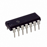
MCP6244-E/P Microchip Technology, MCP6244-E/P Datasheet - Page 8

MCP6244-E/P
Manufacturer Part Number
MCP6244-E/P
Description
IC OPAMP 1.8V QUAD R-R 14DIP
Manufacturer
Microchip Technology
Specifications of MCP6244-E/P
Slew Rate
0.3 V/µs
Amplifier Type
General Purpose
Number Of Circuits
4
Output Type
Rail-to-Rail
Gain Bandwidth Product
550kHz
Current - Input Bias
1pA
Voltage - Input Offset
5000µV
Current - Supply
50µA
Current - Output / Channel
23mA
Voltage - Supply, Single/dual (±)
1.8 V ~ 5.5 V
Operating Temperature
-40°C ~ 125°C
Mounting Type
Through Hole
Package / Case
14-DIP (0.300", 7.62mm)
Op Amp Type
General Purpose
No. Of Amplifiers
4
Bandwidth
550kHz
Supply Voltage Range
1.8V To 5.5V
Amplifier Case Style
DIP
No. Of Pins
14
Operating Temperature Range
-40°C
Number Of Channels
4
Voltage Gain Db
110 dB
Common Mode Rejection Ratio (min)
60 dB
Input Offset Voltage
5 mV
Operating Supply Voltage
3 V, 5 V
Maximum Operating Temperature
+ 125 C
Mounting Style
Through Hole
Minimum Operating Temperature
- 40 C
Lead Free Status / RoHS Status
Lead free / RoHS Compliant
-3db Bandwidth
-
Lead Free Status / Rohs Status
Details
Available stocks
Company
Part Number
Manufacturer
Quantity
Price
Company:
Part Number:
MCP6244-E/P
Manufacturer:
MICROCHIP
Quantity:
12 000
MCP6241/2/4
4.0
The MCP6241/2/4 family of op amps is manufactured
using Microchip’s state-of-the-art CMOS process and
is specifically designed for low-power and general-
purpose applications. The low supply voltage, low
quiescent current and wide bandwidth makes the
MCP6241/2/4 ideal for battery-powered applications.
4.1
The MCP6241/2/4 op amps are designed to prevent
phase reversal when the input pins exceed the supply
voltages. Figure 4-1 shows the input voltage exceeding
the supply voltage without any phase reversal.
FIGURE 4-1:
Phase Reversal.
The input stage of the MCP6241/2/4 op amps use two
differential input stages in parallel. One operates at low
common mode input voltage (V
high V
V
The
V
proper operation.
Input voltages that exceed the input voltage range
(V
excessive current to flow into or out of the input pins.
Current beyond ±2 mA can cause reliability problems.
Applications that exceed this rating must be externally
limited with a resistor, as shown in Figure 4-2.
DS21882C-page 8
CM
CM
SS
up to 300 mV above V
= V
– 0.3V to V
-1
CM
Input
6
5
4
3
2
1
0
SS
APPLICATION INFORMATION
Rail-to-Rail Inputs
. With this topology, the device operates with
– 300 mV and V
Offset
DD
+ 0.3V at 25°C) can cause
The MCP6241/2/4 Show No
V
Time (1 ms/div)
Voltage
IN
DD
DD
V
and 300 mV below V
OUT
CM
+ 300 mV to ensure
is
) and the other at
measured
V
G = +2 V/V
DD
= 5.0V
SS
at
.
FIGURE 4-2:
Resistor (R
4.2
The output voltage range of the MCP6241/2/4 op amps
is V
R
Refer to Figure 2-14 for more information.
4.3
Driving large capacitive loads can cause stability
problems for voltage-feedback op amps. As the load
capacitance increases, the feedback loop’s phase
margin decreases and the closed-loop bandwidth is
reduced. This produces gain peaking in the frequency
response, with overshoot and ringing in the step
response. A unity-gain buffer (G = +1) is the most
sensitive to capacitive loads, but all gains show the
same general behavior.
When driving large capacitive loads with these op
amps (e.g., > 70 pF when G = +1), a small series
resistor at the output (R
feedback loop’s phase margin (stability) by making the
output load resistive at higher frequencies. The
bandwidth will be generally lower than the bandwidth
with no capacitive load.
FIGURE 4-3:
stabilizes large capacitive loads.
Figure 4-4 gives recommended R
different capacitive loads and gains. The x-axis is the
normalized load capacitance (C
circuit’s noise gain. For non-inverting gains, G
signal gain are equal. For inverting gains, G
1 + |Signal Gain| (e.g., –1 V/V gives G
L
V
= 10 k
DD
IN
V
IN
– 35 mV (max.) and V
Rail-to-Rail Output
Capacitive Loads
R
R
IN
IN
is connected to V
IN
–
MCP624X
+
).
------------------------------------------------------------------------------ -
R
V
--------------------------------------------------------------------------- -
Maximum expected V
IN
SS
–
Minimum expected V
Input Current-Limiting
Output resistor, R
ISO
© 2005 Microchip Technology Inc.
–
+
MCP624X
2 mA
2 mA
in Figure 4-3) improves the
SS
R
DD
L
ISO
/G
+ 35 mV (min.) when
/2 and V
C
N
IN
), where G
L
ISO
N
–
= +2 V/V).
V
IN
DD
ISO
DD
values for
N
V
V
= 5.5V.
OUT
N
and the
OUT
is the
N
is


