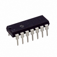
MCP6244-E/P Microchip Technology, MCP6244-E/P Datasheet - Page 10

MCP6244-E/P
Manufacturer Part Number
MCP6244-E/P
Description
IC OPAMP 1.8V QUAD R-R 14DIP
Manufacturer
Microchip Technology
Specifications of MCP6244-E/P
Slew Rate
0.3 V/µs
Amplifier Type
General Purpose
Number Of Circuits
4
Output Type
Rail-to-Rail
Gain Bandwidth Product
550kHz
Current - Input Bias
1pA
Voltage - Input Offset
5000µV
Current - Supply
50µA
Current - Output / Channel
23mA
Voltage - Supply, Single/dual (±)
1.8 V ~ 5.5 V
Operating Temperature
-40°C ~ 125°C
Mounting Type
Through Hole
Package / Case
14-DIP (0.300", 7.62mm)
Op Amp Type
General Purpose
No. Of Amplifiers
4
Bandwidth
550kHz
Supply Voltage Range
1.8V To 5.5V
Amplifier Case Style
DIP
No. Of Pins
14
Operating Temperature Range
-40°C
Number Of Channels
4
Voltage Gain Db
110 dB
Common Mode Rejection Ratio (min)
60 dB
Input Offset Voltage
5 mV
Operating Supply Voltage
3 V, 5 V
Maximum Operating Temperature
+ 125 C
Mounting Style
Through Hole
Minimum Operating Temperature
- 40 C
Lead Free Status / RoHS Status
Lead free / RoHS Compliant
-3db Bandwidth
-
Lead Free Status / Rohs Status
Details
Available stocks
Company
Part Number
Manufacturer
Quantity
Price
Company:
Part Number:
MCP6244-E/P
Manufacturer:
MICROCHIP
Quantity:
12 000
MCP6241/2/4
4.7
4.7.1
To minimize the effect of offset voltage in an amplifier
circuit, the impedances at the inverting and non-
inverting inputs need to be matched. This is done by
choosing the circuit resistor values so that the total
resistance at each input is the same. Figure 4-7 shows
a summing amplifier circuit.
FIGURE 4-7:
To match the inputs, set all voltage sources to ground
and calculate the total resistance at the input nodes. In
this summing amplifier circuit, the resistance at the
inverting input is calculated by setting V
V
parallel. The total resistance at the inverting input is:
At the non-inverting input, V
source. When V
in parallel. The total resistance at the non-inverting
input is:
To minimize offset voltage and increase circuit
accuracy, the resistor values need to meet the
condition:
DS21882C-page 10
OUT
Where:
Where:
V
V
to ground. In this case, R
R
R
IN2
IN1
VIN –
VIN +
Application Circuits
R
R
X
Y
MATCHING THE IMPEDANCE AT
THE INPUTS
V
= total resistance at the inverting input
R
= total resistance at the inverting
DD
R
R
VIN
R
DD
VIN +
input
G1
G2
–
is set to ground, both R
R
R
Z
=
VIN +
=
Summing Amplifier Circuit.
-------------------------------------------- -
⎛
⎝
---------
R
------------------------ -
⎛
⎝
1
------
R
G1
MCP624X
–
+
1
=
X
+
1
+
R
R
VIN
---------
R
DD
----- -
R
F
1
1
1
G1
G2
Y
⎞
⎠
–
, R
is the only voltage
+
+
R
----- -
R
G2
1
Z
F
⎞
⎠
and R
IN1
X
V
and R
, V
OUT
F
IN2
are in
Y
and
are
4.7.2
In analog circuit design, the PCB parasitic capacitance
can compromise the circuit behavior; Figure 4-8 shows
a typical scenario. If the input of an amplifier sees
parasitic capacitance of several picofarad (C
which includes the common mode capacitance of 6 pF,
typical) and large R
of the circuit will include a zero. This parasitic zero
introduces gain peaking and can cause circuit
instability.
FIGURE 4-8:
Capacitance at the Input.
One solution is to use smaller resistor values to push
the zero to a higher frequency. Another solution is to
compensate by introducing a pole at the point at which
the zero occurs. This can be done by adding C
parallel with the feedback resistor (R
selected so that the ratio C
of R
V
V
F
AC
DC
:R
G
.
COMPENSATING FOR THE
PARASITIC CAPACITANCE
C
R
PARA
G
F
and R
Effect of Parasitic
© 2005 Microchip Technology Inc.
MCP624X
+
–
PARA
R
C
G
F
F
, the frequency response
:C
C
F
F
is equal to the ratio
=
F
). C
C
PARA
F
V
needs to be
OUT
R
------ -
R
G
F
PARA
F
in
,


