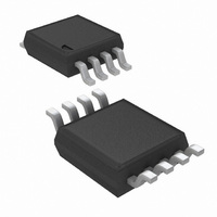
LMV552MM/NOPB National Semiconductor, LMV552MM/NOPB Datasheet - Page 9

LMV552MM/NOPB
Manufacturer Part Number
LMV552MM/NOPB
Description
IC AMP DUAL RR 3MHZ LP 8MSOP
Manufacturer
National Semiconductor
Series
PowerWise®r
Specifications of LMV552MM/NOPB
Amplifier Type
General Purpose
Number Of Circuits
2
Output Type
Rail-to-Rail
Slew Rate
1 V/µs
Gain Bandwidth Product
3MHz
Current - Input Bias
20nA
Voltage - Input Offset
1000µV
Current - Supply
37µA
Current - Output / Channel
25mA
Voltage - Supply, Single/dual (±)
2.7 V ~ 5.5 V
Operating Temperature
-40°C ~ 125°C
Mounting Type
Surface Mount
Package / Case
8-MSOP, Micro8™, 8-uMAX, 8-uSOP,
Bandwidth
3 MHz
Common Mode Rejection Ratio
93
Current, Input Bias
20 nA
Current, Input Offset
1 nA
Current, Output
10 mA
Current, Supply
37 μA
Harmonic Distortion
0.003 %
Impedance, Thermal
235 °C/W
Number Of Amplifiers
Dual
Package Type
MSOP-8
Temperature, Operating, Range
-40 to +125 °C
Voltage, Gain
90 dB
Voltage, Input
2.7 to 5.5 V
Voltage, Noise
70 nV/sqrt Hz
Voltage, Offset
1 mV
Voltage, Output, High
125 mV
Voltage, Output, Low
110 mV
Voltage, Supply
5 V
Number Of Channels
2
Voltage Gain Db
90 dB
Common Mode Rejection Ratio (min)
76 dB
Input Offset Voltage
3 mV at 5 V
Operating Supply Voltage
3 V, 5 V
Supply Current
0.092 mA at 5 V
Maximum Operating Temperature
+ 125 C
Minimum Operating Temperature
- 40 C
Lead Free Status / RoHS Status
Lead free / RoHS Compliant
-3db Bandwidth
-
Lead Free Status / Rohs Status
RoHS Compliant part
Electrostatic Device
Other names
LMV552MMTR
Available stocks
Company
Part Number
Manufacturer
Quantity
Price
Company:
Part Number:
LMV552MM/NOPB
Manufacturer:
National Semiconductor
Quantity:
1 907
Applications Information
ADVANTAGES OF THE LMV551/LMV552/LMV554
Low Voltage and Low Power Operation
The LMV551/LMV552/LMV554 have performance guaran-
teed at supply voltages of 3V and 5V and are guaranteed to
be operational at all supply voltages between 2.7V and 5.5V.
For this supply voltage range, the LMV551/LMV552/LMV554
draw the extremely low supply current of less than 37 μA per
amp.
Wide Bandwidth
The bandwidth to power ratio of 3 MHz to 37 μA per amplifier
is one of the best bandwidth to power ratios ever achieved.
This makes these devices ideal for low power signal process-
ing applications such as portable media players and instru-
mentation.
Low Input Referred Noise
The LMV551/LMV552/LMV554 provide a flatband input re-
ferred voltage noise density of 70 nV/
cantly better than the noise performance expected from an
ultra low power op amp. They also feature the exceptionally
low 1/f noise corner frequency of 4 Hz. This noise specifica-
tion makes the LMV551/LMV552/LMV554 ideal for low power
applications such as PDAs and portable sensors.
Ground Sensing and Rail-to-Rail Output
The LMV551/LMV552/LMV554 each have a rail-to-rail output
stage, which provides the maximum possible output dynamic
range. This is especially important for applications requiring
a large output swing. The input common mode range includes
the negative supply rail which allows direct sensing at ground
in a single supply operation.
Small Size
The small footprints of the LMV551/LMV552/LMV554 pack-
ages save space on printed circuit boards, and enable the
design of smaller and more compact electronic products.
Long traces between the signal source and the op amp make
the signal path susceptible to noise. By using a physically
smaller package, the amplifiers can be placed closer to the
signal source, reducing noise pickup and enhancing signal
integrity
Negative Output Swing vs. Supply Voltage
, which is signifi-
20152638
9
STABILITY OF OP AMP CIRCUITS
Stability and Capacitive Loading
As seen in the Phase Margin vs. Capacitive Load graph, the
phase margin reduces significantly for C
pF. This is because the op amp is designed to provide the
maximum bandwidth possible for a low supply current. Sta-
bilizing them for higher capacitive loads would have required
either a drastic increase in supply current, or a large internal
compensation capacitance, which would have reduced the
bandwidth of the op amp. Hence, if the LMV551/LMV552/
LMV554 are to be used for driving higher capacitive loads,
they will have to be externally compensated.
An op amp, ideally, has a dominant pole close to DC, which
causes its gain to decay at the rate of 20 dB/decade with re-
spect to frequency. If this rate of decay, also known as the
rate of closure (ROC), remains the same until the op amp’s
unity gain bandwidth, the op amp is stable. If, however, a large
capacitance is added to the output of the op amp, it combines
with the output impedance of the op amp to create another
pole in its frequency response before its unity gain frequency
(Figure 1). This increases the ROC to 40 dB/ decade and
causes instability.
FIGURE 1. Gain vs. Frequency for an Op Amp
L
greater than 100
www.national.com
20152603


