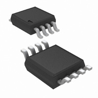
LMV552MM/NOPB National Semiconductor, LMV552MM/NOPB Datasheet - Page 10

LMV552MM/NOPB
Manufacturer Part Number
LMV552MM/NOPB
Description
IC AMP DUAL RR 3MHZ LP 8MSOP
Manufacturer
National Semiconductor
Series
PowerWise®r
Specifications of LMV552MM/NOPB
Amplifier Type
General Purpose
Number Of Circuits
2
Output Type
Rail-to-Rail
Slew Rate
1 V/µs
Gain Bandwidth Product
3MHz
Current - Input Bias
20nA
Voltage - Input Offset
1000µV
Current - Supply
37µA
Current - Output / Channel
25mA
Voltage - Supply, Single/dual (±)
2.7 V ~ 5.5 V
Operating Temperature
-40°C ~ 125°C
Mounting Type
Surface Mount
Package / Case
8-MSOP, Micro8™, 8-uMAX, 8-uSOP,
Bandwidth
3 MHz
Common Mode Rejection Ratio
93
Current, Input Bias
20 nA
Current, Input Offset
1 nA
Current, Output
10 mA
Current, Supply
37 μA
Harmonic Distortion
0.003 %
Impedance, Thermal
235 °C/W
Number Of Amplifiers
Dual
Package Type
MSOP-8
Temperature, Operating, Range
-40 to +125 °C
Voltage, Gain
90 dB
Voltage, Input
2.7 to 5.5 V
Voltage, Noise
70 nV/sqrt Hz
Voltage, Offset
1 mV
Voltage, Output, High
125 mV
Voltage, Output, Low
110 mV
Voltage, Supply
5 V
Number Of Channels
2
Voltage Gain Db
90 dB
Common Mode Rejection Ratio (min)
76 dB
Input Offset Voltage
3 mV at 5 V
Operating Supply Voltage
3 V, 5 V
Supply Current
0.092 mA at 5 V
Maximum Operating Temperature
+ 125 C
Minimum Operating Temperature
- 40 C
Lead Free Status / RoHS Status
Lead free / RoHS Compliant
-3db Bandwidth
-
Lead Free Status / Rohs Status
RoHS Compliant part
Electrostatic Device
Other names
LMV552MMTR
Available stocks
Company
Part Number
Manufacturer
Quantity
Price
Company:
Part Number:
LMV552MM/NOPB
Manufacturer:
National Semiconductor
Quantity:
1 907
www.national.com
In such a case a number of techniques can be used to restore
stability to the circuit. The idea behind all these schemes is to
modify the frequency response such that it can be restored to
an ROC of 20 dB/decade, which ensures stability.
In the Loop Compensation
Figure 2 illustrates a compensation technique, known as ‘in
the loop’ compensation, that employs an RC feedback circuit
within the feedback loop to stabilize a non-inverting amplifier
configuration. A small series resistance, R
the amplifier output from the load capacitance, C
capacitance, C
bypass C
The values for R
zero attributed to C
attributed to C
pole on the transfer function is compensated for by the pres-
ence of the zero, and that the ROC is maintained at 20 dB/
decade. For the circuit shown in Figure 2 the values of R
C
maintaining stability for different values of C
phase margins obtained, are shown in Table 1. R
R
Although this methodology provides circuit stability for any
load capacitance, it does so at the price of bandwidth. The
closed loop bandwidth of the circuit is now limited by R
C
Compensation by External Resistor
In some applications it is essential to drive a capacitive load
without sacrificing bandwidth. In such a case, in the loop com-
pensation is not viable. A simpler scheme for compensation
F
L
F
.
are given by Equation 1. Values of R
are to be 10 kΩ, while R
C
L
100
150
50
(pF)
L
FIGURE 2. In the Loop Compensation
at higher frequencies.
L
F
. This ensures that the effect of the second
, is inserted across the feedback resistor to
S
R
and C
340
340
340
S
F
(Ω)
lies at the same frequency as the pole
TABLE 1.
F
are decided by ensuring that the
OUT
C
is 340Ω.
F
15
22
8
(pF)
S
and C
S
, is used to isolate
Phase Margin
L
, as well as the
L
F
, and a small
required for
20152604
F
(°)
47
42
40
, R
IN
F
S
, and
and
and
(1)
10
is shown in Figure 3. A resistor, R
tween the load capacitance and the output. This introduces a
zero in the circuit transfer function, which counteracts the ef-
fect of the pole formed by the load capacitance and ensures
stability. The value of R
pending on the size of C
sired. Values ranging from 5Ω to 50Ω are usually sufficient to
ensure stability. A larger value of R
with less ringing and overshoot, but will also limit the output
swing and the short circuit current of the circuit.
Typical Application
ACTIVE FILTERS
With a wide unity gain bandwidth of 3 MHz, low input referred
noise density and a low power supply current, the LMV551/
LMV552/LMV554 are well suited for low-power filtering appli-
cations. Active filter topologies, such as the Sallen-Key low
pass filter shown in Figure 4, are very versatile, and can be
used to design a wide variety of filters (Chebyshev, Butter-
worth or Bessel). The Sallen-Key topology, in particular, can
be used to attain a wide range of Q, by using positive feed-
back to reject the undesired frequency range.
In the circuit shown in Figure 4, the two capacitors appear as
open circuits at lower frequencies and the signal is simply
buffered to the output. At high frequencies the capacitors ap-
pear as short circuits and the signal is shunted to ground by
one of the capacitors before it can be amplified. Near the cut-
off frequency, where the impedance of the capacitances is on
the same order as R
other capacitor allows the circuit to attain the desired Q.
FIGURE 3. Compensation by Isolation Resistor
FIGURE 4. Sallen-Key Filter
G
and R
ISO
L
to be used should be decided de-
and the level of performance de-
F
, positive feedback through the
ISO
ISO
, is placed in series be-
will result in a system
20152612
20152609


