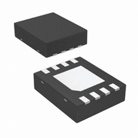
LMH6553SDE/NOPB National Semiconductor, LMH6553SDE/NOPB Datasheet - Page 22

LMH6553SDE/NOPB
Manufacturer Part Number
LMH6553SDE/NOPB
Description
IC AMP DIFF 900MHZ W/CLAMP 8LLP
Manufacturer
National Semiconductor
Series
LMH®, PowerWise®r
Datasheet
1.LMH6553SDENOPB.pdf
(26 pages)
Specifications of LMH6553SDE/NOPB
Amplifier Type
Differential
Number Of Circuits
1
Output Type
Differential
Slew Rate
2300 V/µs
-3db Bandwidth
900MHz
Current - Input Bias
50µA
Current - Supply
29.1mA
Current - Output / Channel
120mA
Voltage - Supply, Single/dual (±)
4.5 V ~ 12 V, ±2.25 V ~ 6 V
Operating Temperature
-40°C ~ 125°C
Mounting Type
Surface Mount
Package / Case
8-LLP
No. Of Amplifiers
1
Bandwidth
900MHz
Supply Voltage Range
4.5V To 12V
Supply Current
29.1mA
Amplifier Case Style
LLP
No. Of Pins
8
Rohs Compliant
Yes
Lead Free Status / RoHS Status
Lead free / RoHS Compliant
Gain Bandwidth Product
-
Voltage - Input Offset
-
Other names
*LMH6553SDE/NOPB
LMH6553SDETR
LMH6553SDETR
www.national.com
POWER DISSIPATION
The LMH6553 is optimized for maximum speed and perfor-
mance in the small form factor of the standard LLP package.
To ensure maximum output drive and highest performance,
thermal shutdown is not provided. Therefore, it is of utmost
importance to make sure that the T
ceeded.
Follow these steps to determine the maximum power dissi-
pation for the LMH6553:
1.
2.
3.
The maximum power that the LMH6553 package can dissi-
pate at a given temperature can be derived with the following
equation:
P
(°C) and θ
MAX
FIGURE 14. Single Supply Bypassing Capacitors
Calculate the quiescent (no-load) power: P
V
through the feedback network if V
Calculate the RMS power dissipated in each of the output
stages: P
− V
and the current measured at the output pins of the
differential amplifier as if they were single ended
amplifiers and V
Calculate the total RMS power: P
FIGURE 13. Split Supply Bypassing Capacitors
= (150° – T
S
, where V
−
OUT
JA
) * I
= Thermal resistance, from junction to ambient,
D
(rms) = rms ((V
−
AMB
S
OUT
= V
)/ θ
) , where V
S
+
is the total supply voltage.
JA
- V
, where T
−
. (Be sure to include any current
S
OUT
- V
AMB
JMAX
and I
+
OUT
= Ambient temperature
T
CM
of 150°C is never ex-
) * I
= P
OUT
is not mid-rail.)
AMP
+
30043701
are the voltage
OUT
30043712
AMP
+ P
) + rms ((V
D
= I
.
CC
*
S
22
for a given package (°C/W). For the PSOP package θ
59°C/W; LLP package θ
NOTE: If V
rent flowing in the feedback network. This current should be
included in the thermal calculations and added into the qui-
escent power dissipation of the amplifier.
THERMAL PERFORMANCE
The LMH6553 is available in both the PSOP and LLP pack-
ages. Both packages are designed for enhanced thermal
performance and features an exposed die attach pad (DAP)
at the bottom center of the package that creates a direct path
to the PCB for maximum power dissipation. The DAP is float-
ing and is not electrically connected to internal circuitry.
The thermal advantage of the two packages is fully realized
only when the exposed die attach pad is soldered down to a
thermal land on the PCB board with thermal vias planted un-
derneath the thermal land. The thermal land can be connect-
ed to any power or ground plane within the allowable supply
voltage range of the device. The junction-to-ambient thermal
resistance (θ
as opposed to an alternative with no direct soldering to a ther-
mal land. Based on thermal analysis of the LLP package, the
junction-to-ambient thermal resistance (θ
by a factor of two when the die attach pad of the LLP package
is soldered directly onto the PCB with thermal land and ther-
mal vias are 1.27 mm and 0.33 mm respectively. Typical
copper via barrel plating is 1 oz, although thicker copper may
be used to further improve thermal performance.
For more information on board layout techniques for the LLP
package, refer to Application Note 1187 “Leadless Lead
Frame Package (LLP).” This application note also discusses
package handling, solder stencil and the assembly process.
ESD PROTECTION
The LMH6553 is protected against electrostatic discharge
(ESD) on all pins. The LMH6553 will survive 4000V Human
Body model and 350V Machine model events. Under normal
operation the ESD diodes have no effect on circuit perfor-
mance. The current that flows through the ESD diodes will
either exit the chip through the supply pins or through the de-
vice, hence it is possible to power up a chip with a large signal
applied to the input pins.
BOARD LAYOUT
The LMH6553 is a very high performance amplifier. In order
to get maximum benefit from the differential circuit architec-
ture, board layout and component selection are very critical.
The circuit board should have a low inductance ground plane
and well bypassed wide supply lines. External components
should be leadless surface mount types. The feedback net-
work and output matching resistors should be composed of
short traces and precision resistors (0.1%). The output match-
ing resistors should be placed within 3 or 4 mm of the amplifier
as should the supply bypass capacitors. Refer to the section
titled Power Supply Bypassing for recommendations on by-
pass circuit layout. Evaluation boards are available free of
charge through the product folder on National’s web site.
By design, the LMH6553 is relatively insensitive to parasitic
capacitance at its inputs. Nonetheless, ground and power
plane metal should be removed from beneath the amplifier
and from beneath R
frequency.
With any differential signal path, symmetry is very important.
Even small amounts of asymmetry can contribute to distortion
and balance errors.
CM
JA
is not mid-rail, then there will be quiescent cur-
) of the LMH6553 can be significantly lowered,
F
and R
JA
is 58°C/W.
G
for best performance at high
JA
) can be improved
JA
is


