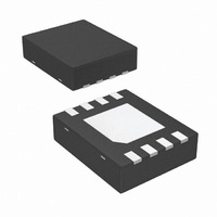
LMH6553SD/NOPB National Semiconductor, LMH6553SD/NOPB Datasheet

LMH6553SD/NOPB
Specifications of LMH6553SD/NOPB
Related parts for LMH6553SD/NOPB
LMH6553SD/NOPB Summary of contents
Page 1
... PSOP and 8-pin LLP packages, and is part of our LMH ® high speed amplifier family. Typical Application LMH ® registered trademark of National Semiconductor Corporation. © 2010 National Semiconductor Corporation LMH6553 Features ■ 900 MHz −3 dB small signal bandwidth @ A ■ 670 MHz −3 dB large signal bandwidth @ A ■ ...
Page 2
... Absolute Maximum Ratings If Military/Aerospace specified devices are required, please contact the National Semiconductor Sales Office/ Distributors for availability and specifications. ESD Tolerance (Note 5) Human Body Model Machine Model Supply Voltage Common Mode Input Voltage Maximum Input Current (pins Maximum Output Current (pins 4, 5) ...
Page 3
Symbol Parameter Input Characteristics I Input Bias Current (Note 11 Input Bias Current Differential Boffset (Note 7) CMRR Common Mode Rejection Ratio (Note 7) R Input Resistance IN C Input Capacitance IN CMVR Input Common Mode Voltage Range ...
Page 4
Symbol Parameter V Output Common Mode Error OSCM Input Bias Current Voltage Range CMRR Input Resistance Gain Miscellaneous Performance Z Open Loop Transimpedance T PSRR Power Supply Rejection Ratio I Supply Current ±2.5V Electrical Characteristics S Unless ...
Page 5
Symbol Parameter Noise Figure (See Figure 5) Input Characteristics I Input Bias Current (Note 11 Input Bias Current Differential Boffset (Note 7) CMRR Common Mode Rejection Ratio (Note 7) R Input Resistance IN C Input Capacitance IN CMVR ...
Page 6
Symbol Parameter V Output Common Mode Error OSCM Input Bias Current Voltage Range CMRR Input Resistance Gain Miscellaneous Performance Z Open Loop Transimpedance T PSRR Power Supply Rejection Ratio I Supply Current S Note 1: Absolute Maximum Ratings indicate limits ...
Page 7
Connection Diagrams Pin Descriptions Pin No. Pin Name Description 1 -IN Negative Input 2 V Output Common Mode Control Positive Supply 4 +OUT Positive Output 5 -OUT Negative Output 6 V- Negative Supply 7 V Output Voltage ...
Page 8
Typical Performance Characteristics V for single ended in, differential out, unless specified). Frequency Response vs. Gain Frequency Response vs. V Frequency Response vs. Supply Voltage (R www.national.com = ± 25° Frequency Response vs. Gain 30043747 ...
Page 9
Frequency Response vs. Capacitive Load Frequency Response vs. Resistive Load Frequency Response vs Suggested R 30043721 Frequency Response vs. Resistive Load 30043759 1 V Pulse Response Single-Ended Input PP 30043761 9 vs. Capacitive Load O 30043722 30043760 30043726 ...
Page 10
V Pulse Response Single-Ended Input PP Pulse Response with 0% and 100% Overdrive Overdrive Recovery with V www.national.com 4 V Pulse Response Single-Ended Input PP 30043727 Pulse Response with 0% and 100% Overdrive 30043774 = ±5V Overdrive Recovery with ...
Page 11
Output Common Mode Pulse Response Distortion vs. Supply Voltage (f =20Mhz Distortion vs =20Mhz Distortion vs. Frequency Single-Ended Input (R 30043724 =800Ω) Distortion vs. Supply Voltage (f L 30043743 =800Ω) Distortion vs. V ...
Page 12
Distortion vs. Frequency Single-Ended Input (R Distortion vs. Supply Voltage (f Distortion vs =75Mhz www.national.com =200Ω) Distortion vs. Supply Voltage (f L 30043781 =200Ω) =75Mhz, R Distortion vs 30043783 =200Ω) L 30043785 ...
Page 13
Minimum V vs. I OUT OUT 30043731 Closed Loop Output Impedance 30043718 Open Loop Transimpedance 30043742 Closed Loop Output Impedance Open Loop Transimpedance PSRR 13 30043717 30043741 30043719 www.national.com ...
Page 14
PSRR Balance Error Noise Figure www.national.com 30043720 Noise Figure 30043713 Differential S-Parameter Magnitude vs. Frequency 30043746 14 CMRR 30043733 30043745 30043755 ...
Page 15
Differential S-Parameter Phase vs. Frequency 3rd Order Intermodulation Products vs. V 3rd Order Intermodulation Products vs. Center Frequency 3rd Order Intermodulation Products vs. V 30043756 3rd Order Intermodulation Products vs. Center Frequency OUT 30043752 3rd Order Intermodulation Products vs. Center ...
Page 16
Order Intermodulation Products vs. Center Frequency www.national.com 3rd Order Intermodulation Products vs. V 30043779 16 CLAMP 30043780 ...
Page 17
Application Information The LMH6553, a fully differential current feedback amplifier with integrated output common mode control and output lim- iting clamp, is designed to provide protection of following input stages. The common mode feedback circuit sets the output common mode ...
Page 18
FIGURE 3. Single-Ended Input with Differential Output When using the LMH6553 in single-to-differential mode, the complementary output is forced to a phase inverted replica of the driven output by the common mode feedback circuit as opposed to being driven by ...
Page 19
SPLIT SUPPLY OPERATION For optimum performance, split supply operation is recom- mended using +5V and −5V supplies; however, operation is possible on split supplies as low as +2.25V and −2.25V and as high as +6V and −6V. Provided the total ...
Page 20
OUTPUT NOISE PERFORMANCE AND MEASUREMENT Unlike differential amplifiers based on voltage feedback ar- chitectures, noise sources internal to the LMH6553 refer to the inputs largely as current sources, hence the low input re- ferred voltage noise and relatively higher input ...
Page 21
High Speed Differential Amplifiers to Drive ADCs. For more information regarding a particular ADC, refer to the particular ADC datasheet for details. TABLE 3. DIFFERENTIAL INPUT ADCs COMPATIBLE WITH LMH6553 DRIVER Product Number Max Resolution Sampling Rate (MSPS) ADC1173 15 ...
Page 22
FIGURE 13. Split Supply Bypassing Capacitors FIGURE 14. Single Supply Bypassing Capacitors POWER DISSIPATION The LMH6553 is optimized for maximum speed and perfor- mance in the small form factor of the standard LLP package. To ensure maximum output drive and ...
Page 23
EVALUATION BOARD See the LMH6553 Product Folder on www.national.com for evaluation board availability and ordering information. 23 www.national.com ...
Page 24
Physical Dimensions www.national.com inches (millimeters) unless otherwise noted 8-Pin PSOP NS Package Number MRA08A 8-Pin LLP NS Package Number SDA08C 24 ...
Page 25
Notes 25 www.national.com ...
Page 26
... For more National Semiconductor product information and proven design tools, visit the following Web sites at: www.national.com Products Amplifiers www.national.com/amplifiers Audio www.national.com/audio Clock and Timing www.national.com/timing Data Converters www.national.com/adc Interface www.national.com/interface LVDS www.national.com/lvds Power Management www.national.com/power Switching Regulators www.national.com/switchers LDOs www.national.com/ldo LED Lighting www ...


