LF444CM/NOPB National Semiconductor, LF444CM/NOPB Datasheet - Page 3
LF444CM/NOPB
Manufacturer Part Number
LF444CM/NOPB
Description
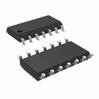
IC OP AMP QUAD LOPWR JFET 14SOIC
Manufacturer
National Semiconductor
Series
BI-FET™r
Type
General Purpose Amplifierr
Specifications of LF444CM/NOPB
Amplifier Type
J-FET
Number Of Circuits
4
Slew Rate
1 V/µs
Gain Bandwidth Product
1MHz
Current - Input Bias
10pA
Voltage - Input Offset
3000µV
Current - Supply
600µA
Voltage - Supply, Single/dual (±)
10 V ~ 36 V, ±5 V ~ 18 V
Operating Temperature
0°C ~ 70°C
Mounting Type
Surface Mount
Package / Case
14-SOIC (3.9mm Width), 14-SOL
Bandwidth
1 MHz
Channel Separation
-120
Common Mode Rejection Ratio
95
Current, Input Bias
10 pA
Current, Input Offset
5 pA
Current, Output
8 mA
Current, Supply
0.6 mA
Impedance, Thermal
85 °C/W
Number Of Amplifiers
Quad
Package Type
SOIC-14
Power Dissipation
670 mW
Resistance, Input
10^12 Ohms
Temperature, Operating, Range
0 to +70 °C
Voltage, Gain
100 V/mV
Voltage, Input
6 to 44 V
Voltage, Noise
35 nV/sqrt Hz
Voltage, Offset
2 mV
Voltage, Output, High
13 V
Voltage, Output, Low
-13 V
Voltage, Supply
±15 V
Rail/rail I/o Type
No
Number Of Elements
4
Unity Gain Bandwidth Product
1MHz
Input Offset Voltage
10@±15VmV
Input Bias Current
100pA
Single Supply Voltage (typ)
Not RequiredV
Dual Supply Voltage (typ)
±5/±9/±12/±15V
Voltage Gain In Db
100dB
Power Supply Rejection Ratio
70dB
Power Supply Requirement
Dual
Shut Down Feature
No
Single Supply Voltage (min)
Not RequiredV
Single Supply Voltage (max)
Not RequiredV
Dual Supply Voltage (min)
±3V
Dual Supply Voltage (max)
±18V
Technology
BiFET
Operating Temp Range
0C to 70C
Operating Temperature Classification
Commercial
Mounting
Surface Mount
Pin Count
14
Lead Free Status / RoHS Status
Lead free / RoHS Compliant
Output Type
-
Current - Output / Channel
-
-3db Bandwidth
-
Lead Free Status / Rohs Status
RoHS Compliant part
Electrostatic Device
Other names
*LF444CM
*LF444CM/NOPB
LF444CM
*LF444CM/NOPB
LF444CM


SR
GBW
e
i
Symbol
n
n
AC Electrical Characteristics
Note 1: Unless otherwise specified the absolute maximum negative input voltage is equal to the negative power supply voltage.
Note 2: Any of the amplifier outputs can be shorted to ground indefinitely, however, more than one should not be simultaneously shorted as the maximum junction
temperature will be exceeded.
Note 3: For operating at elevated temperature, these devices must be derated based on a thermal resistance of θ
Note 4: The LF444A is available in both the commercial temperature range 0˚C ≤ T
is available in the commercial temperature range only. The temperature range is designated by the position just before the package type in the device number. A
“C” indicates the commercial temperature range and an “M” indicates the military temperature range. The military temperature range is available in “D” package only.
Note 5: Unless otherwise specified the specifications apply over the full temperature range and for V
V
Note 6: The input bias currents are junction leakage currents which approximately double for every 10˚C increase in the junction temperature, T
production test time, the input bias currents measured are correlated to junction temperature. In normal operation the junction temperature rises above the ambient
temperature as a result of internal power dissipation, P
recommended if input bias current is to be kept to a minimum.
Note 7: Supply voltage rejection ratio is measured for both supply magnitudes increasing or decreasing simultaneously in accordance with common practice from
Note 8: Refer to RETS444X for LF444MD military specifications.
Note 9: Max. Power Dissipation is defined by the package characteristics. Operating the part near the Max. Power Dissipation may cause the part to operate outside
guaranteed limits.
Note 10: Human body model, 1.5 kΩ in series with 100 pF.
Note 11: Absolute Maximum Ratings indicate limits beyond which damage to the device may occur. Operating ratings indicate conditions for which the device is
functional, but do not guarantee specific performance limits. Electrical Characteristics state DC and AC electrical specifications under particular test conditions which
guarantee specific performance limits. This assumes that the device is within the Operating Ratings. Specifications are not guaranteed for parameters where no limit
is given, however, the typical value is a good indication of device performance.
Typical Performance Characteristics
±
OS
15V to
, I
B
, and I
±
Amplifier-to-Amplifier
Coupling
Slew Rate
Gain-Bandwidth Product
Equivalent Input Noise Voltage
Equivalent Input Noise Current
5V for the LF444 and from
OS
are measured at V
Parameter
Input Bias Current
CM
±
= 0.
20V to
±
5V for the LF444A.
V
V
T
f = 1 kHz
T
D
A
A
. T
S
S
00915612
=
=
= 25˚C, R
= 25˚C, f = 1 kHz
j
= T
(Note 5)
±
±
Conditions
15V, T
15V, T
A
+ θ
jA
P
S
A
A
D
= 100Ω,
= 25˚C
= 25˚C
where θ
3
A
jA
≤ 70˚C and the military temperature range −55˚C ≤ T
is the thermal resistance from junction to ambient. Use of a heat sink is
Min
LF444A
−120
0.01
Typ
35
S
1
1
=
±
20V for the LF444A and for V
Max
Input Bias Current
jA
.
Min
LF444
−120
0.01
Typ
35
1
1
Max
S
=
A
±
≤ 125˚C. The LF444
00915613
15V for the LF444.
j
. Due to limited
www.national.com
Units
V/µs
MHz
dB
Related parts for LF444CM/NOPB
Image
Part Number
Description
Manufacturer
Datasheet
Request
R

Part Number:
Description:
IC, OP-AMP, 1MHZ, 1V/µs, SOIC-14
Manufacturer:
National Semiconductor
Datasheet:

Part Number:
Description:
National Semiconductor [8-Bit D/A Converter]
Manufacturer:
National Semiconductor
Datasheet:
Part Number:
Description:
National Semiconductor [Media Coprocessor]
Manufacturer:
National Semiconductor
Datasheet:
Part Number:
Description:
Digitally Controlled Tone and Volume Circuit with Stereo Audio Power Amplifier, Microphone Preamp Stage and National 3D Sound
Manufacturer:
National Semiconductor
Datasheet:
Part Number:
Description:
Digitally Controlled Tone and Volume Circuit with Stereo Audio Power Amplifier, Microphone Preamp Stage and National 3D Sound
Manufacturer:
National Semiconductor
Datasheet:
Part Number:
Description:
AC97 Rev 2 Codec with Sample Rate Conversion and National 3D Sound
Manufacturer:
National Semiconductor
Part Number:
Description:
Manufacturer:
National Semiconductor
Datasheet:
Part Number:
Description:
Manufacturer:
National Semiconductor
Datasheet:
Part Number:
Description:
General Purpose, Low Voltage, Low Power, Rail-to-Rail Output Operational Amplifiers
Manufacturer:
National Semiconductor
Datasheet:
Part Number:
Description:
8-bit 20 MSPS flash A/D converter.
Manufacturer:
National Semiconductor
Datasheet:
Part Number:
Description:
Low Noise Quad Operational Amplifier
Manufacturer:
National Semiconductor
Datasheet:
Part Number:
Description:
Quad Differential Line Receivers
Manufacturer:
National Semiconductor
Datasheet:
Part Number:
Description:
Quad High Speed Trapezoidal? Bus Transceiver
Manufacturer:
National Semiconductor
Datasheet:
Part Number:
Description:
Dual Line Receiver
Manufacturer:
National Semiconductor
Datasheet: