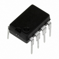
LF442CN/NOPB National Semiconductor, LF442CN/NOPB Datasheet - Page 2

LF442CN/NOPB
Manufacturer Part Number
LF442CN/NOPB
Description
IC OP AMP DUAL LO PWR JFET 8-DIP
Manufacturer
National Semiconductor
Series
BI-FET II™r
Specifications of LF442CN/NOPB
Amplifier Type
J-FET
Number Of Circuits
2
Slew Rate
1 V/µs
Gain Bandwidth Product
1MHz
Current - Input Bias
10pA
Voltage - Input Offset
1000µV
Current - Supply
400µA
Voltage - Supply, Single/dual (±)
10 V ~ 36 V, ±5 V ~ 18 V
Operating Temperature
0°C ~ 70°C
Mounting Type
Through Hole
Package / Case
8-DIP (0.300", 7.62mm)
Bandwidth
1 MHz
Channel Separation
-120
Common Mode Rejection Ratio
95
Current, Input Bias
10 pA
Current, Input Offset
5 pA
Current, Output
6.8 mA
Current, Supply
400 μA
Impedance, Thermal
152 °C/W
Number Of Amplifiers
Dual
Package Type
MDIP-8
Resistance, Input
10^12 Ohms
Temperature, Operating, Range
0 to +70 °C
Voltage, Gain
200 V/mV
Voltage, Input
6 to 44 V
Voltage, Noise
35 nV/sqrt Hz
Voltage, Offset
1 mV
Voltage, Output, High
13 V
Voltage, Output, Low
-13 V
Voltage, Supply
±15 V
Lead Free Status / RoHS Status
Lead free / RoHS Compliant
Output Type
-
Current - Output / Channel
-
-3db Bandwidth
-
Lead Free Status / Rohs Status
RoHS Compliant part
Electrostatic Device
Other names
*LF442CN
*LF442CN/NOPB
LF442
LF442CN
*LF442CN/NOPB
LF442
LF442CN
www.national.com
V
∆V
I
I
R
A
V
V
CMRR
PSRR
I
OS
B
S
Symbol
OS
VOL
O
CM
IN
Absolute Maximum Ratings
If Military/Aerospace specified devices are required,
please contact the National Semiconductor Sales Office/
Distributors for availability and specifications.
DC Electrical Characteristics
T
Supply Voltage
Differential Input Voltage
Input Voltage Range
Output Short Circuit
OS
j
(Note 2)
Duration (Note 3)
max
/∆T
Input Offset Voltage
Average TC of Input
Offset Voltage
Input Offset Current
Input Bias Current
Input Resistance
Large Signal Voltage
Gain
Output Voltage Swing
Input Common-Mode
Voltage Range
Common-Mode
Rejection Ratio
Supply Voltage
Rejection Ratio
Supply Current
Parameter
H Package
150˚C
Continuous
LF442A
±
±
±
R
Over Temperature
R
V
(Notes 7, 8)
V
(Notes 7, 8)
T
V
R
Over Temperature
V
R
(Note 9)
22V
38V
19V
j
S
S
S
S
S
S
L
S
= 25˚C
= 10 kΩ, T
=
=
=
=
= 10 kΩ, T
= 10 kΩ
≤ 10 kΩ
±
±
±
±
15V
15V
15V, V
15V, R
N Package
Continuous
(Note 1)
115˚C
Conditions
LF442
(Note 7)
±
±
±
O
L
A
A
18V
30V
15V
= 10 kΩ
=
= 25˚C
= 25˚C
±
10V,
T
T
T
T
T
T
j
j
j
j
j
j
= 25˚C
= 70˚C
= 125˚C
= 25˚C
= 70˚C
= 125˚C
2
θ
θ
Operating Temperature
Storage
Lead Temperature
ESD Tolerance
JA
JC
(Note 4)
(Note 5)
Range
Temperature Range
(Soldering, 10 sec.)
(Typical)
(Typical)
Min
±
±
50
25
80
80
12
16
LF442A
10
Typ
±
200
200
+18
−17
100
100
300
0.5
10
7
5
13
12
Max
400
1.0
1.5
10
25
10
50
20
−65˚C≤T
3
H Package
165˚C/W
(Note 5)
65˚C/W
21˚C/W
Rating to be determined
260˚C
±
±
Min
25
15
70
70
12
11
A
≤150˚C−65˚C≤T
LF442
10
Typ
±
+14
−12
200
200
400
1.0
10
95
90
7
5
13
12
N Package
114˚C/W
152˚C/W
Max
(Note 5)
100
500
5.0
7.5
1.5
50
260˚C
3
A
≤150˚C
Units
µV/˚C
V/mV
V/mV
mV
mV
pA
nA
nA
pA
nA
nA
dB
dB
µA
Ω
V
V
V


