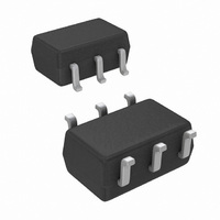
LMH6601MG/NOPB National Semiconductor, LMH6601MG/NOPB Datasheet - Page 6

LMH6601MG/NOPB
Manufacturer Part Number
LMH6601MG/NOPB
Description
IC AMP VFA 2.4V SHUTDOWN SC70-6
Manufacturer
National Semiconductor
Datasheet
1.LMH6601MGNOPB.pdf
(28 pages)
Specifications of LMH6601MG/NOPB
Amplifier Type
Voltage Feedback
Number Of Circuits
1
Output Type
Rail-to-Rail
Slew Rate
275 V/µs
Gain Bandwidth Product
155MHz
-3db Bandwidth
250MHz
Current - Input Bias
5pA
Voltage - Input Offset
1000µV
Current - Supply
9.6mA
Current - Output / Channel
180mA
Voltage - Supply, Single/dual (±)
2.4 V ~ 5.5 V, ±1.2 V ~ 2.75 V
Operating Temperature
-40°C ~ 85°C
Mounting Type
Surface Mount
Package / Case
SC-70-6, SC-88, SOT-363
Number Of Channels
1
Voltage Gain Db
66 dB
Common Mode Rejection Ratio (min)
56 dB
Input Offset Voltage
2.4 mV at 5 V
Operating Supply Voltage
3 V, 5 V
Supply Current
11.5 mA at 5 V
Maximum Operating Temperature
+ 85 C
Minimum Operating Temperature
- 40 C
For Use With
LMH730227 - BOARD EVALUATION FOR SOIC PKGLMH730165 - BOARD EVALUATIONLMH730216 - BOARD EVAL HS MONO AMP SOT23
Lead Free Status / RoHS Status
Lead free / RoHS Compliant
Other names
LMH6601MG
LMH6601MGTR
LMH6601MGTR
www.national.com
Frequency Domain Response
SSBW
SSBW_1
Peak
Peak_1
LSBW
Peak_2
0.1 dB BW
GBWP_1k
GBWP_150
A
PBW
DG
DP
Time Domain Response
TRS/TRL
OS
SR
T
T
PD
Distortion & Noise Performance
HD2
HD3
V
V
I
Static, DC Performance
V
DV
I
I
R
C
+PSRR
−PSRR
CMRR
CMVR
N
B
OS
S
S_1
VOL
N1
N2
IO
IN
IN
2.7V Electrical Characteristics
V
Symbol
IO
S
/2, R
L
= 150Ω to V
–3 dB Bandwidth Small Signal
Peaking
Peaking
–3 dB Bandwidth Large Signal
Peaking
0.1 dB Bandwidth
Gain Bandwidth Product
Large Signal Open Loop Gain
Full Power BW
Differential Gain
Differential Phase
Rise & Fall Time
Overshoot
Slew Rate
Settling Time
Propagation Delay
Harmonic Distortion (2
Harmonic Distortion (3
Input Voltage Noise
Input Current Noise
Input Offset Voltage
Input Offset Voltage Average Drift
Input Bias Current
Input Offset Current
Input Resistance
Input Capacitance
Positive Power Supply Rejection
Ratio
Negative Power Supply Rejection
Ratio
Common Mode Rejection Ratio
Input Voltage Range
−
unless otherwise specified. Boldface limits apply at temperature extremes.
Parameter
nd
rd
)
)
V
V
V
V
V
V
V
Unity Gain, R
Unity Gain, R
0.25V < V
–1 dB, A
R
4.43 MHz, 0.45V
R
4.43 MHz, 0.45V
R
0.25V Step
0.25V Step
2V Step
1V Step, ±0.1%
1V Step, ±0.02%
Input to Output, 250 mV Step, 50%
1 V
1 V
>10 MHz
1 MHz
>1 MHz
(Note
(Note
(Note
0V
DC
DC
DC
CMRR > 50 dB
OUT
OUT
OUT
OUT
OUT
OUT
OUT
L
L
L
= 150Ω to V
= 150Ω to V
= 150Ω to V
PP
PP
≤
Single Supply with V
= 0.25 V
= 0.25 V
= 0.25 V
= 0.25 V
= 2 V
= 2 V
= 2V
, 10 MHz
, 10 MHz
V
8)
9)
9)
IN
V
≤
OUT
PP
= +4, V
PP
PP
1.2V
L
L
PP
PP
PP
PP
< 2.5V
Condition
= 1 kΩ to V
= 150Ω to V
S
−
−
6
, A
, A
/2
≤
≤
OUT
V
V
V
V
= +1
= +1
OUT
OUT
= 2 V
≤
≤
S
S
S
PP
/2
2.05V
2.05V
= 2.7V, A
/2
,
V
= +2, R
(Note
V
−
Min
56
58
53
56
53
57
52
-0.20
F
6)
= 604Ω, SD tied to V
(Note
(Note
0.12
0.62
−6.5
Typ
120
250
110
260
147
410
−58
−60
3.1
0.1
2.7
3.4
8.4
1.6
±1
73
30
81
65
13
10
12
50
20
68
69
77
0
5
2
–
2)
6)
(Note
V
Max
±3.5
±6.5
+
50
25
-1.5
+
6)
, V
OUT
nV/
fA/
Units
μV/°C
MHz
MHz
MHz
MHz
MHz
V/μs
deg
dBc
dBc
mV
TΩ
=
dB
dB
dB
dB
pA
pA
pF
dB
dB
dB
ns
ns
ns
%
%
V


