LMV721M7/NOPB National Semiconductor, LMV721M7/NOPB Datasheet - Page 4
LMV721M7/NOPB
Manufacturer Part Number
LMV721M7/NOPB
Description
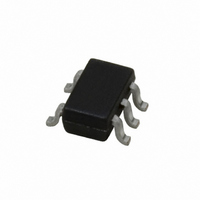
IC OP AMP LOW VOLT LP SC-70-5
Manufacturer
National Semiconductor
Series
PowerWise®r
Datasheet
1.LMV721M7NOPB.pdf
(16 pages)
Specifications of LMV721M7/NOPB
Amplifier Type
General Purpose
Number Of Circuits
1
Output Type
Rail-to-Rail
Slew Rate
5.25 V/µs
Gain Bandwidth Product
10MHz
Current - Input Bias
260nA
Voltage - Input Offset
80µV
Current - Supply
1.03mA
Current - Output / Channel
52.6mA
Voltage - Supply, Single/dual (±)
2.2 V ~ 5.5 V, ±1.1 V ~ 2.25 V
Operating Temperature
-40°C ~ 85°C
Mounting Type
Surface Mount
Package / Case
SC-70-5, SC-88A, SOT-323-5, SOT-353, 5-TSSOP
Number Of Channels
1
Voltage Gain Db
94 dB
Common Mode Rejection Ratio (min)
70 dB
Input Offset Voltage
3 mV at 5 V
Operating Supply Voltage
3 V, 5 V
Supply Current
1.4 mA at 5 V
Maximum Operating Temperature
+ 85 C
Minimum Operating Temperature
- 40 C
Lead Free Status / RoHS Status
Lead free / RoHS Compliant
-3db Bandwidth
-
Lead Free Status / Rohs Status
Details
Other names
LMV721M7
LMV721M7TR
LMV721M7TR
Available stocks
Company
Part Number
Manufacturer
Quantity
Price


www.national.com
SR
GBW
Φ
G
e
i
THD
n
n
m
m
5V AC Electrical Characteristics
Unless otherwise specified, all limits guaranteed for T
Boldface limits apply at the temperature extremes.
Note 1: Absolute Maximum Ratings indicate limits beyond which damage to the device may occur. Operating Ratings indicate conditions for which the device is
intended to be functional, but specific performance is not guaranteed. For guaranteed specifications and the test conditions, see the Electrical Characteristics.
Note 2: Human body model, 1.5 kΩ in series with 100 pF. Machine model, 200Ω in series with 100 pF.
Note 3: Applies to both single-supply and split-supply operation. Continuous short circuit operation at elevated ambient temperature can result in exceeding the
maximum allowed junction temperature of 150°C. Output currents in excess of 30 mA over long term may adversely affect reliability.
Note 4: The maximum power dissipation is a function of T
P
Note 5: Typical Values represent the most likely parametric norm.
Note 6: All limits are guaranteed by testing or statistical analysis.
Note 7: Connected as voltage follower with 1V step input. Number specified is the slower of the positive and negative slew rate.
Symbol
D
= (T
J(max)
–T
Slew Rate
Gain-Bandwidth Product
Phase Margin
Gain Margin
Input-Related Voltage Noise
Input-Referred Current Noise
Total Harmonic Distortion
A
)/θ
JA
. All numbers apply for packages soldered directly into a PC board.
Parameter
J(max)
, θ
JA
J
(Note 7)
f = 1 kHz
f = 1 kHz
f = 1kHz, A
R
, and T
= 25°C. V
L
= 600Ω, V
A
. The maximum allowable power dissipation at any ambient temperature is
4
+
V
= 5V, V
= 1
O
Conditions
= 1 V
−
PP
= 0V, V
CM
= V
+
/2, V
O
= V
+
/2 and R
(Note 5)
0.001
5.25
10.0
Typ
−11
8.5
0.2
72
L
> 1 MΩ.
Units
V/μs
MHz
Deg
dB
%
Related parts for LMV721M7/NOPB
Image
Part Number
Description
Manufacturer
Datasheet
Request
R

Part Number:
Description:
IC, OP-AMP, 10MHZ, 5.25V/µs, SC-70-5
Manufacturer:
National Semiconductor
Datasheet:

Part Number:
Description:
National Semiconductor [8-Bit D/A Converter]
Manufacturer:
National Semiconductor
Datasheet:
Part Number:
Description:
National Semiconductor [Media Coprocessor]
Manufacturer:
National Semiconductor
Datasheet:
Part Number:
Description:
Digitally Controlled Tone and Volume Circuit with Stereo Audio Power Amplifier, Microphone Preamp Stage and National 3D Sound
Manufacturer:
National Semiconductor
Datasheet:
Part Number:
Description:
Digitally Controlled Tone and Volume Circuit with Stereo Audio Power Amplifier, Microphone Preamp Stage and National 3D Sound
Manufacturer:
National Semiconductor
Datasheet:
Part Number:
Description:
AC97 Rev 2 Codec with Sample Rate Conversion and National 3D Sound
Manufacturer:
National Semiconductor
Part Number:
Description:
Manufacturer:
National Semiconductor
Datasheet:
Part Number:
Description:
Manufacturer:
National Semiconductor
Datasheet:
Part Number:
Description:
General Purpose, Low Voltage, Low Power, Rail-to-Rail Output Operational Amplifiers
Manufacturer:
National Semiconductor
Datasheet:
Part Number:
Description:
8-bit 20 MSPS flash A/D converter.
Manufacturer:
National Semiconductor
Datasheet:
Part Number:
Description:
Low Noise Quad Operational Amplifier
Manufacturer:
National Semiconductor
Datasheet:
Part Number:
Description:
Quad Differential Line Receivers
Manufacturer:
National Semiconductor
Datasheet:
Part Number:
Description:
Quad High Speed Trapezoidal? Bus Transceiver
Manufacturer:
National Semiconductor
Datasheet:
Part Number:
Description:
Dual Line Receiver
Manufacturer:
National Semiconductor
Datasheet: