LPV511MG/NOPB National Semiconductor, LPV511MG/NOPB Datasheet - Page 5
LPV511MG/NOPB
Manufacturer Part Number
LPV511MG/NOPB
Description
IC OP AMP 880NA R-R SC70-5
Manufacturer
National Semiconductor
Series
PowerWise®r
Datasheet
1.LPV511MGNOPB.pdf
(14 pages)
Specifications of LPV511MG/NOPB
Amplifier Type
General Purpose
Number Of Circuits
1
Output Type
Rail-to-Rail
Slew Rate
0.0077 V/µs
Gain Bandwidth Product
25kHz
Current - Input Bias
320pA
Voltage - Input Offset
200µV
Current - Supply
1.2µA
Current - Output / Channel
1.3mA
Voltage - Supply, Single/dual (±)
2.7 V ~ 12 V
Operating Temperature
-40°C ~ 85°C
Mounting Type
Surface Mount
Package / Case
SC-70-5, SC-88A, SOT-323-5, SOT-353, 5-TSSOP
Number Of Channels
1
Voltage Gain Db
110 dB
Common Mode Rejection Ratio (min)
80 dB
Input Voltage Range (max)
12 V
Input Voltage Range (min)
2.7 V
Input Offset Voltage
3 mV at 5 V
Operating Supply Voltage
3 V, 5 V, 9 V
Supply Current
0.0012 mA at 5 V
Maximum Operating Temperature
+ 85 C
Mounting Style
SMD/SMT
Minimum Operating Temperature
- 40 C
Lead Free Status / RoHS Status
Lead free / RoHS Compliant
-3db Bandwidth
-
Lead Free Status / Rohs Status
Details
Other names
LPV511MG
LPV511MGNOPB
LPV511MGNOPBTR
LPV511MGNOPBTR
LPV511MGTR
LPV511MGNOPB
LPV511MGNOPBTR
LPV511MGNOPBTR
LPV511MGTR


Note 1: Absolute Maximum Ratings indicate limits beyond which damage to the device may occur. Operating Ratings indicate conditions for which the device is
intended to be functional, but specific performance is not guaranteed. For guaranteed specifications and the test conditions, see the Electrical Characteristics
Tables.
Note 2: Human Body Model: 1.5 kΩ in series with 100 pF. Machine Model: 0Ω in series with 200 pF.
Note 3: The maximum power dissipation is a function of T
P
Note 4: Output short circuit duration is infinite for V
Note 5: Electrical table values apply only for factory testing conditions at the temperature indicated. Factory testing conditions result in very limited self-heating
of the device.
Note 6: Limits are 100% production tested at 25°C. Limits over the operating temperature range are guaranteed through correlations using the Statistical Quality
Control (SQC) method.
Note 7: Typical values represent the most likely parametric norm at the time of characterization.
Note 8: Offset voltage drift is guaranteed by design and/or characterization and is not tested in production. Offset voltage drift is determined by dividing the change
in V
Note 9: Positive current corresponds to current flowing into the device.
Note 10: The Short Circuit Test is a momentary test. See
Note 11: Slew rate is the average of the rising and falling slew rates.
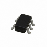
Connection Diagram
Ordering Information
D
= (T
OS
5-Pin SC70
Package
at temperature extremes into the total temperature change.
J(MAX)
- T
A
)/ θ
JA
. All numbers apply for packages soldered directly onto a PC board.
Part Number
LPV511MGX
LPV511MG
+
< 6V at room temperature and below. For V
(Note 4)
J(MAX)
Package Marking
, θ
JA
, and T
.
A91
Top View
SC70-5
A
. The maximum allowable power dissipation at any ambient temperature is
5
20117001
1k Units Tape and Reel
3k Units Tape and Reel
+
> 6V, allowable short circuit duration is 1.5 ms.
Transport Media
NSC Drawing
MA005A
www.national.com
Related parts for LPV511MG/NOPB
Image
Part Number
Description
Manufacturer
Datasheet
Request
R

Part Number:
Description:
Manufacturer:
National Semiconductor
Datasheet:
Part Number:
Description:
IC,Operational Amplifier,SINGLE,BIPOLAR,TSSOP,6PIN,PLASTIC
Manufacturer:
National Semiconductor
Part Number:
Description:
National Semiconductor [8-Bit D/A Converter]
Manufacturer:
National Semiconductor
Datasheet:
Part Number:
Description:
National Semiconductor [Media Coprocessor]
Manufacturer:
National Semiconductor
Datasheet:
Part Number:
Description:
Digitally Controlled Tone and Volume Circuit with Stereo Audio Power Amplifier, Microphone Preamp Stage and National 3D Sound
Manufacturer:
National Semiconductor
Datasheet:
Part Number:
Description:
Digitally Controlled Tone and Volume Circuit with Stereo Audio Power Amplifier, Microphone Preamp Stage and National 3D Sound
Manufacturer:
National Semiconductor
Datasheet:
Part Number:
Description:
AC97 Rev 2 Codec with Sample Rate Conversion and National 3D Sound
Manufacturer:
National Semiconductor
Part Number:
Description:
Manufacturer:
National Semiconductor
Datasheet:
Part Number:
Description:
Manufacturer:
National Semiconductor
Datasheet:
Part Number:
Description:
General Purpose, Low Voltage, Low Power, Rail-to-Rail Output Operational Amplifiers
Manufacturer:
National Semiconductor
Datasheet:
Part Number:
Description:
8-bit 20 MSPS flash A/D converter.
Manufacturer:
National Semiconductor
Datasheet:
Part Number:
Description:
Low Noise Quad Operational Amplifier
Manufacturer:
National Semiconductor
Datasheet:
Part Number:
Description:
Quad Differential Line Receivers
Manufacturer:
National Semiconductor
Datasheet:
Part Number:
Description:
Quad High Speed Trapezoidal? Bus Transceiver
Manufacturer:
National Semiconductor
Datasheet: