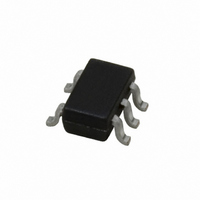
LPV511MG/NOPB National Semiconductor, LPV511MG/NOPB Datasheet - Page 4

LPV511MG/NOPB
Manufacturer Part Number
LPV511MG/NOPB
Description
IC OP AMP 880NA R-R SC70-5
Manufacturer
National Semiconductor
Series
PowerWise®r
Datasheet
1.LPV511MGNOPB.pdf
(14 pages)
Specifications of LPV511MG/NOPB
Amplifier Type
General Purpose
Number Of Circuits
1
Output Type
Rail-to-Rail
Slew Rate
0.0077 V/µs
Gain Bandwidth Product
25kHz
Current - Input Bias
320pA
Voltage - Input Offset
200µV
Current - Supply
1.2µA
Current - Output / Channel
1.3mA
Voltage - Supply, Single/dual (±)
2.7 V ~ 12 V
Operating Temperature
-40°C ~ 85°C
Mounting Type
Surface Mount
Package / Case
SC-70-5, SC-88A, SOT-323-5, SOT-353, 5-TSSOP
Number Of Channels
1
Voltage Gain Db
110 dB
Common Mode Rejection Ratio (min)
80 dB
Input Voltage Range (max)
12 V
Input Voltage Range (min)
2.7 V
Input Offset Voltage
3 mV at 5 V
Operating Supply Voltage
3 V, 5 V, 9 V
Supply Current
0.0012 mA at 5 V
Maximum Operating Temperature
+ 85 C
Mounting Style
SMD/SMT
Minimum Operating Temperature
- 40 C
Lead Free Status / RoHS Status
Lead free / RoHS Compliant
-3db Bandwidth
-
Lead Free Status / Rohs Status
Details
Other names
LPV511MG
LPV511MGNOPB
LPV511MGNOPBTR
LPV511MGNOPBTR
LPV511MGTR
LPV511MGNOPB
LPV511MGNOPBTR
LPV511MGNOPBTR
LPV511MGTR
www.national.com
i
V
TC V
I
I
CMRR
PSRR
CMVR
A
V
I
I
SR
GBW
e
i
n
n
B
OS
SC
S
Symbol
Symbol
n
OS
VOL
O
12V Electrical Characteristics
Unless otherwise specified, all limits are guaranteed for T
Boldface limits apply to the temperature range of −40°C to 85°C.
OS
Input-Referred Current Noise
Input Offset Voltage
Input Offset Voltage Drift
Input Bias Current (Note 9)
Input Offset Current
Common Mode Rejection Ratio
Power Supply Rejection Ratio
Input Common-Mode Voltage
Range
Large Signal Voltage Gain
Output Swing High
Output Swing Low
Output Short Circuit Current (Note
10)
Supply Current
Slew Rate (Note 11)
Gain Bandwidth Product
Phase Margin
Input-Referred Voltage Noise
Input-Referred Current Noise
Parameter
Parameter
f = 10 Hz
f = 1 kHz
(Note 8)
V
V
V
V
V
V
V
V
CMRR
Sinking, V
Sourcing, V
V
V
Sourcing
V
Sinking
V
A
R
R
f = 100 Hz
f = 10 Hz
f = 1 kHz
CM
CM
CM
CM
CM
+
+
+
ID
ID
ID
ID
V
L
L
= 2.7V to 5V, V
= 3V to 5V, V
= 5V to 12V, V
= +1, V
= 1 MΩ, C
= 1 MΩ, C
= 100 mV
= −100 mV
= 100 mV
= −100 mV
Stepped from 0V to +6V
Stepped from 11.4V to 12V
Stepped from 0.5V to 11.5
= 0.5V
= 11.5V
(Note 5)
≥
50 dB
O
O
O
= 0.5V
ramped from 1V to 11V
J
= 11.5V
L
L
= 25°C, V
= 50 pF
= 50 pF
Conditions
Conditions
CM
CM
CM
4
= 0.5V
= 0.5V
= 0.5V
+
= 12V, V
−
= 0V, V
CM
(Note 6)
(Note 6)
−1000
−1600
11.72
−0.1
11.8
5.25
3.10
= V
Min
Min
200
75
70
75
68
70
65
72
68
76
72
84
80
89
84
0
O
= V
+
(Note 7)
(Note 7)
/2, and R
11.85
−320
−650
1300
±0.2
±0.3
Typ
Typ
110
±10
115
110
114
115
117
110
150
320
.02
.01
1.2
7.0
.02
.01
97
25
52
L
(Note 6)
(Note 6)
= 100 kΩ to V
1900
−200
Max
Max
±3.8
12.1
1.75
±15
800
200
280
2.5
±3
12
pA/
nV/
pA/
μV/°C
Units
Units
V/ms
kHz
deg
mV
mV
pA
pA
dB
dB
dB
μA
μA
+
V
V
/2.


